I see so many misconceptions about BJTs, people seem to either over-complicate the hell out of them, or over-simplify and then wonder why things don’t work. I want to find a nice middle point, something overcomplicated that doesn’t work.
Today’s post is to build a simple ground-up understanding of the BJT using fun analogies that gives you insight into how it works on an atomic scale, and work our way up to a model that allows us to actually make useful circuits on a macro scale.

Battle of the Bands
Silicon is among the most well understood elements on the periodic table after oxygen, carbon, and the element of surprise. A silicon atom is, like any atom, comprised of a nucleus with protons and neutrons surrounded by electrons.
Silicon has 14 protons and 14 electrons. That’s equal, neutral charge. Remember that it is charge neutral, this will keep coming up in our understanding. In its natural state it forms a crystal. That doesn’t mean it looks like a gemstone, it looks more like a ball of aluminum foil, but the molecules form a lattice structure, a strong even grid, like an atomic phalanx.
The electrons face a conundrum. They are strongly attracted to the protons at the center, but cannot stand being next to each other. They come to an agreement where they will arrange themselves in such a way as to not step on each others’ toes. This ends up creating “bands” of electrons around the nucleus. Each band is further away from the nucleus and therefore has more space to house more electrons.
The two outer bands of the greatest interest to us are the valence band and conduction band.

See, as one atom gets more and more electrons, they just move out to further and further bands as expected. But atoms don’t exist in isolation. They have other atoms around them and form structures. Those electrons can play more complex games to stay away from each other while staying close to a nucleus. Valence band electrons start to feel because they’re now so far away from their nucleus’s protons, but they can make up for it by being shared with adjacent atoms. Conduction electrons however are like free spirits, shared between the whole structure, among all atoms in the crystal. The way they “move” through the crystal even has a momentum and wavelength, which is beyond what we’ll discuss here.
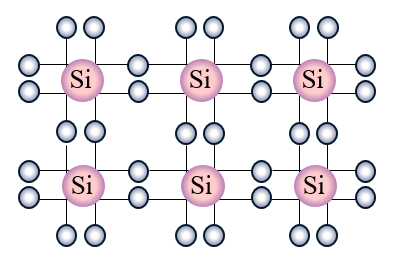
Those “free” electrons in the conduction band are what’s of interest to us as circuit designers, since that’s all that’s available for us to work with. When we talk about “P-type” or “N-type” silicon later on, we’re not talking about silicon that is positively or negatively charged, we’re talking about silicon that has greater or fewer free electrons and thus appear positively or negatively charged from a conduction band perspective. This is in sharp contrast to metals, which are unique in that *all* their electrons are in the conduction band, making them great conductors.

This might seem like way too much detail. Why are we going this far inside an individual atom to describe the behavior of a device you can hold in your hands? Because the operation of a BJT is all about what parts are charged and how they are or aren’t charged. We’ll dispell some misconceptions students have when learning this that make it tough to understand.
Dopesick
Silicon itself has certain properties, it has 14 protons and electrons and has a mass and such. By itself it has somewhat useful properties. But there’s something really amazing about it, which is that we can change its properties by adding other elements to it in the right concentrations. And if we add the right elements in the right concentrations, we can then apply the right voltages to make it do all sorts of stuff!
Remember that the most useful band to us is the conduction band. Silicon is atomic number 14, so the most relevant elements are boron and phosphorous, because they are elements 13 and 15 respectively. That’s the number of protons they have, but when neutrally charged it’s also the number of electrons. What happens if we mix some boron or phosphorous into the silicon? It changes the possible free electrons in the conduction band.
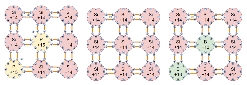
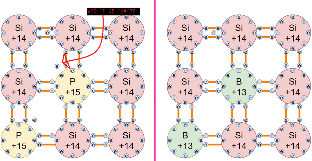
Below are side by side graphics of a silicon structure where one of the atoms is replaced with phosphorous, and another where one atom is replaced with boron. If you count up the total number of free electrons, you’ll see phosphorous has an extra electron which will have to go into the conduction band. If you look at the one on the right, you’ll see boron is missing an electron, it has -1 free electrons. In fact we go so far as to call this lack of electron a charge carrier in and of itself, a “hole”, a positive charge. Read our post on electrons and holes here for more details. Nevertheless, in both cases, the structures are entirely charge neutral because the total number of electrons including the lower level ones not shown is equal to the total number of protons in the nuclei. We simply ignore those and abstract it away. Remember this.
The Depletion Region: the DMZ of semiconductors
Imagine a big potluck for the neighborhood at the community center. Everyone in the neighborhood is invited, all sorts of families. The only rule is that they must bring one dish for every family member. So a family of 3 brings 3 dishes. Lasagna, biryani, and tiramisu (title of my memoir).

Unfortunately the potluck is organized by Martha. And Martha is…well her heart is in the right place. She’s seating everyone and she says half the families will go here, and half the families over on the other side of the hall. But she makes no accounting for the fact that different families are different sizes. Most families have 4 people, but some have 3, some have 5. Somehow all the families of 3 end up seated on the left side, while families of 5 are on the right.
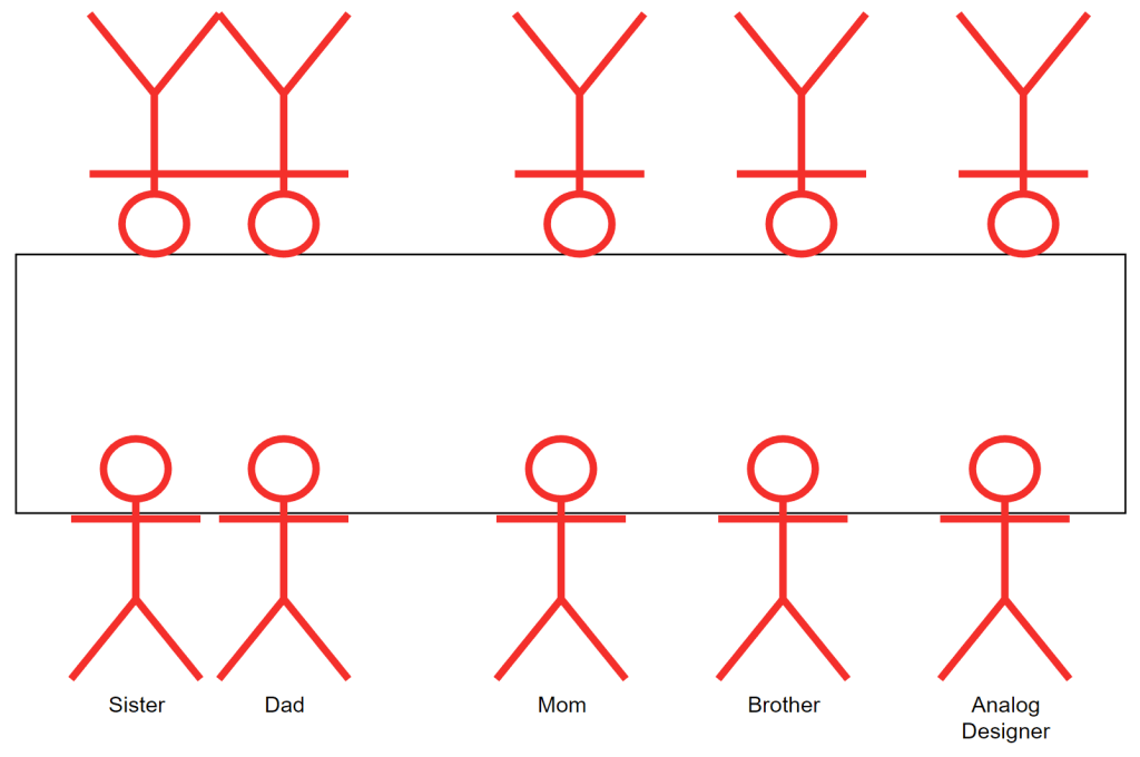
A curious thing happens. There is one dish per person distributed perfectly around the hall, but an uneven number of dishes on either side in absolute terms. The people sitting at the table only see one side has more food than the other, so by instinct they just start passing dishes from the side with more people to the side with fewer people.
People sitting at the middle though catch on pretty quickly, and they stop passing. The table has reached an “equilibrium point” that is far from clean. It’s a mess, now around the middle some people are getting too little food, and others too much. Think about that, it’s “settled” overall even though it’s obviously not.
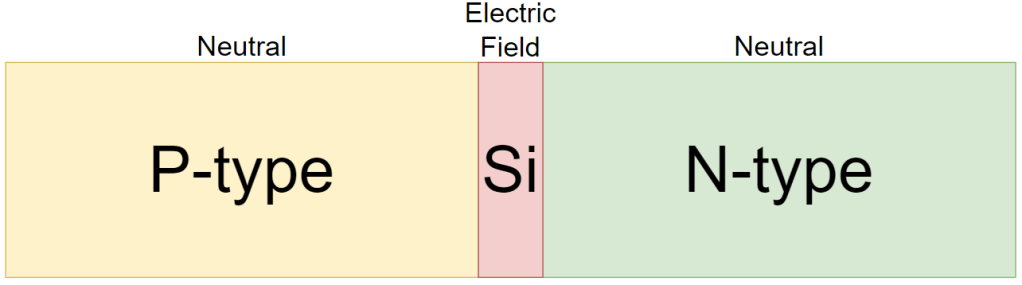
This controlled mess is what’s at the heart of a “PN junction” and a lot of silicon physics/engineering. It’s natural state is kind of in disarray. It’s certainly *not* what Martha wanted. When you take silicon as-is, and then add boron or phosphorous to it, you change the number of apparent electrons (dishes) even though the number of electrons matches the number of protons (families). Phosphorous has extra electrons so we call the phosphorous-doped silicon N-type for negative, and boron has fewer electrons so we call boron-doped silicon P-type for positive. Again, they are both charge neutral, it’s only their outer bands that appear to have positive or negative charge. When you then put them together they mistakenly think they are out of equilibrium and create a new equilibrium that normally would not be possible. That middle section which is charged and has an electric field is called the ‘depletion region”. For anything to occur, you have to first overcome this false balance, to “replenish” the depletion region. If you leave it as is, or apply voltage in the wrong direction, current is blocked and it looks like an insulator. Only when you apply the right voltage in the right direction do they conduct. Thus….semi-conductor.
Stuck In The Middle With You
A PN junction (also known as a diode) is when we put a P-type and N-type material together. If you apply a voltage difference across that junction, you can counter the effects of the “organized chaos” and conduct current. We can take this to the next level by putting another N-type material on the other side of the P-type, so now we have a P-type sandwiched between two N-types, known as an NPN. Okay guys, settle down, I know some of you know what’s coming and are already cheering and jumping in the air. Yes yes, the moment is finally here.

This is a BJT, or bipolar junction transistor. How do we expect current to flow? From one N to another? We’ve established that the PN junction blocks current flow unless you apply a voltage across it from P to N. We could tie the P high, and both N’s low, but that wouldn’t be particularly useful would it? Might as well just put two diodes in parallel. If we tie one N high, and the other N to ground, and the P somewhere in the middle, current should flow from the P to the lower N, but nothing would flow from the upper N down, right? That makes the upper PN junction useless…right?
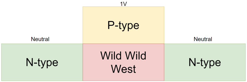
Let’s go over what happens in this scenario. The P-type portion we call the base. The lower N-type we call the emitter and upper N-type the collector, for reasons that will become clear. When we apply a voltage across the base-emitter PN junction, we overcome the depletion region, we reverse that “false equilibrium”. The emitter emits electrons and sends them to fill the holes in the base.
Here is trick #1 of the NPN BJT. In a typical diode, the P and N types are doped with roughly equal concentrations, so you get an equal exchange of electrons into holes. It’s nice that way. In this scenario, we wayyyy over-dope the emitter compared to the base. The base wants it’s holes filled and makes all sorts of promises to the emitter. Hey emitter, come on, send your electrons over, I have sooo much space for them!

The base is kind of a slimeball. It is obviously lying, and the emitter sends all these electrons, but suddenly finds itself in a predicament. Not only are there not that many holes to fill because the base is doped less than the emitter, but the base is tiny!
This is trick #2 of the NPN BJT. The excess electrons don’t find themselves nestled in the vast empty space of the rest of the base, they are crammed and shoved and within moments find themselves in a terrible spot: the upper PN junction. Forgot about that junction didn’t you? The upper N-type, i.e. the collector, is at a higher voltage, which means that PN junction still has its depletion region. Remember what I said about the depletion region. It is not charge neutral, it has an electric field. What do electric fields do? They are defined entirely by how they move charge. Take a charged object, put it in an electric field, that shit will flyyyy.
We can imagine the electrons from the emitter like canoes rowing to safety in the docks of the base. But there are only so many docks, the emitter sends too many based on the false promises of the base. Not only that, but there’s a storm and large current (haha get it?) just past the base. All the poor lost extra electrons from the emitter get swept up in that current, and are launched through the collector out the other side. The collector collects the excess electrons emitted by the emitter, who missed the base where the docks are.
From a circuits perspective, since we only consider the movement of positive charges, it looks to us like if we create a small current from base to emitter, we get a large current from collector to emitter.
And that’s basically it! There’s more to it, there’s other regions of operation, but this is the main interesting mechanism. If you can understand why/how this works, you are pretty much ready to understand the rest of it. Getting your head around this part is the main difficulty, from there it’s pretty straightforward.
 Positive Feedback