The transistor will go down as one of the most consequential inventions in history, behind agriculture, paper, and the Super Soaker. But on the list of inventions that have completely transformed the very fabric of the human condition, it showed up pretty late in the game, and that’s because it’s a fairly complex thing. Conceptually complex, but much harder to actually create and implement.
Safe to say that it takes some time to get to know these buggers, learning new contexts and new perspectives that unlock new capabilities. As I see it, here are the 5 stages of understanding transistors, from beginner to expert. These aren’t mutually exclusive, sometimes stage 1 thinking is the best way to approach it, other times stage 4.
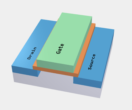
Stage 1: Transistors are a switch
Your first understanding of transistors is that you can switch something on and off with a voltage instead of physically flipping a switch. You can turn a light or motor on or off by just typing 1 or 0 and hitting Enter.

You put more switches together in complex configurations, and you get logic. Once you get logic, now you’re in the world of Claude Shannon. Suddenly, the entire world of logic becomes available to you. Any level of logic is possible with these 1’s and 0’s. Like 95% or more of all semiconductors out in the world today are used as switches. “On”, or “Off”. 1 or 0. See how switches turn into computers and software in this article.
Now at this stage the concept is pretty simple but even here there’s practical effects to watch out for. It’s not a perfect switch, it has some resistance, it burns power particularly during the transition. The gate is basically a capacitor so that might need to be driven by a dedicated circuit. That gives you a time constant, propagation delay, and so forth. But at the abstract level this is simple stuff.

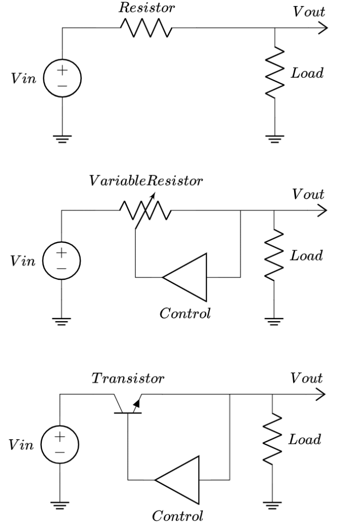
Stage 2: Transistors are a variable resistor
I mentioned the transition during switching and its resistance. Well let’s dwell on that.
If the switch is off, that’s the same as being an open circuit, or an infinite Ohm resistor. If the switch is on, it’s a short circuit, or a zero Ohm resistor. If there’s a transition, that must mean that the transistor can be some resistance between zero and infinite.
That resistance is actually controllable. The input of the transistor doesn’t have to go all the way, if you bring it above a threshold value (a few hundred millivolts) you can make the transistor act like a variable resistor, with a finite value up to you.
If it’s in series with another resistor, that means you can also pull a variable amount of current through that resistor, and you have a variable voltage divider. We’re starting to move from digital into the analog domain and things are starting to heat up a little.
Here’s a simple application, if you have one voltage and want to convert to another, you can divide it down. But this only works if the load is constant. If the load, the bottom resistor of the voltage divider, changes, then the output voltage also changes. Well then what if we had a way to make the top resistor variable? A potentiometer? No then you’d have to sit there fiddling with it, not to mention you’d have no way to deal with with noise or quick spikes in current. A transistor, when thought of as an electronically variable resistor, works perfectly here. What you see below is in fact a linear voltage regulator, which exists in some form in almost every electronic device today.
Unfortunately, we start to find that this resistance control is not as linear as we’d like. As the voltage across it increases, the current also increases until suddenly it hits a wall and doesn’t increase any further, it saturates. Let’s hold onto that.
Stage 3: Transistors are non-linear voltage-controlled current sources
This is where we move really move into the domain of analog design. From a circuit theory perspective, a transistor is fundamentally a transconductance device. That means it converts a voltage to a current. In fact the very word “transistor” is short for “transconductance resistor“.
You convert the voltage to a current, and then hook that current up to a resistor to turn it into a voltage, and bam you’ve got a voltage amplifier! It goes the other way too, you can convert a current to a voltage with one transistor, and convert that voltage to a current with another transistor, which is a current amplifier or current mirror. A simple back-and-forth combination of this is how op-amps are made.

Voltage to current, current to voltage. As long as we end up with a bigger number than we started with, we have an amplifier. This forms the basis of most analog microelectronics and is about where you end up with an undergrad education in microelectronics.
But once again, this behavior is highly non-linear. We break the transistor’s circuit behavior into distinct “regions of operation” like saturation or triode in the standard Charge Sheet Model (CSM), or weak/moderate/strong inversion in the EKV model. There are low frequency and high frequency models where we take things like parasitic capacitance into account, and second and third order effects like, channel-length modulation, body effect, Miller capacitance, and so on. It can get out of hand but we can model all of these things with fundamental circuit elements like resistors and current sources, until we hit a bit of a limit.
Stage 4: Transistors are charge-controlled 3-dimensional semiconductor structures, where charge on one surface affects the channel inversion and mobility, subject to electromagnetic fields and thermal effects
Houston, we have lift off. This is where we fly away from circuit theory entirely and move to a physics-based understanding of MOSFETs.
The current moving through the transistor is moving through a semiconductor with charge carriers induced in it. The properties of that channel are based on its doping, purity, the Fermi level, temperature, etc. Charge on the gate affects these properties and induces mobile charge carriers through an inversion layer. None of this is captured in a circuit schematic. The drain and source form pn junctions with depletion regions with the substrate. There’s drift current and diffusion current. None of this is captured in a circuit schematic. At very high frequencies, your signals are not just signals, they’re electromagnetic waves propagating through and reflecting off a mish-mash of conductors and insulators and semiconductors. None of this is captured in a circuit schematic. If your transistors are arranged in such a way that those pn junctions are in just the wrong spot, they form a network of BJTs without you even knowing and can create a positive feedback loop that crashes the circuit called “latch-up”. This is definitely not captured in a circuit schematic.
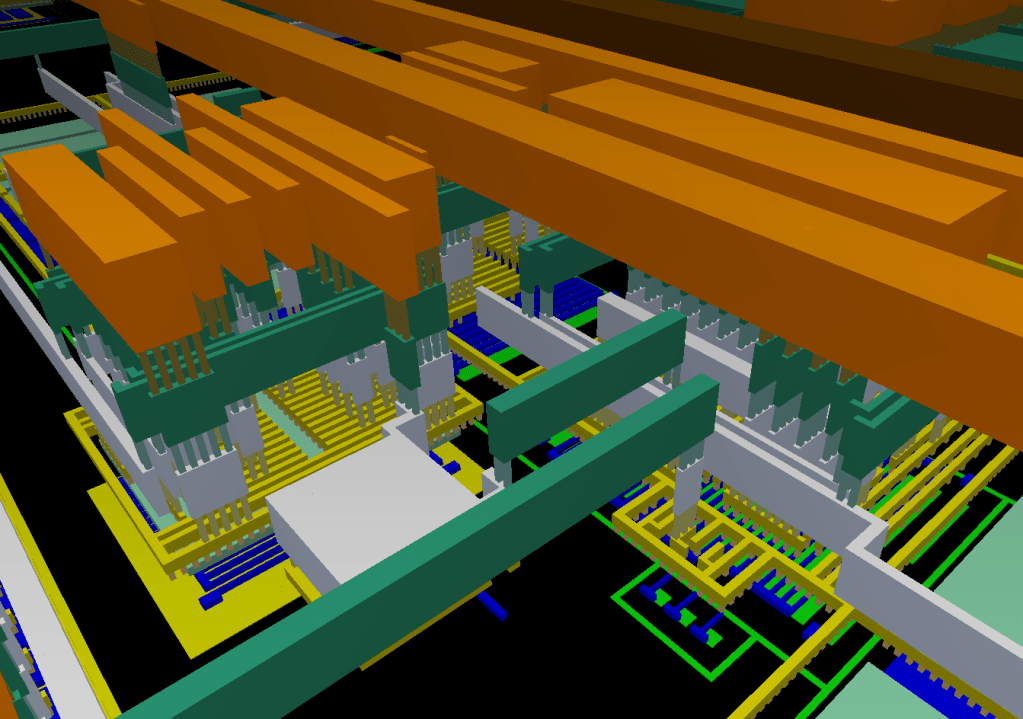
The picture below is a very zoomed-in 3D rendering of an comparator I laid out. Do you see a small-signal model anywhere? Do you see a current mirror? Do you see any ground symbols? In the end this is what is actually fabricated, metal and silicon smaller than a micrometer. This is what actually gets packaged up and soldered into a system, the real physical thing, and it has to live in the harsh physical world where its out in the cold or gets dropped into the toilet.
A proper understanding of the actual physics gives you a proper understanding of the circuit model and its abstractions and what it actually means and what you can and can’t assume based on it. The physics understanding is what allows you to prevent issues like latch-up. The physics understanding is what allows you to exploit its temperature dependence and create biasing circuits and control loops that are stable across temperature, as well as the ever-stable bandgap reference that billions and billions of devices rely on.
But the physics understanding is so dense and opaque that it becomes unwieldy for most design. After all that’s why nobody uses Maxwell’s equations directly for circuit design, thanks to people like Charles Proteus Steinmetz. There’s a whole field built around properly capturing physics effects in abstract circuit models, called “compact modeling”.
Stage 5: All of the above
The reality is that every one of these perspectives is useful in different situations, some more than others, and depending quite a bit on the process. A standard MOSFET in a 350nm process does not operate the same as a power transistor in a BCD (BJT, CMOS, DMOS) process, which does not operate like a 7nm FinFET. You need all of these perspectives and know when and how to employ them.
Different types of designers need to know different parts better. Digital VLSI designers know how to use the first two stages with such precision that they can predict precisely down to femtoseconds how digital signals will travel through millions of transistor switches and meet logic timing requirements. RF designers are living (or dying, depending on the day) between stage 3 and 4, considering things like voltage gain and bias conditions from a circuit perspective while also thinking about s-parameters and how the inductors in their oscillators radiate and couple energy into their amplifiers. Semiconductor physicists and fabrication experts live almost exclusively in stage 4. Power electronics designers employ all stages equally to make high power resonant converters.
Whichever stage you use most often or are most comfortable with, try venturing out and seeing how occupying another stage opens up new ways of thinking. Happy transresisting!

This article taught me more than one semester of PCB design/entry-level electronics in my CS class in barely 5 minutes. Honestly this website is a life-saver, thanks for actually taking your time to write these articles.
LikeLike