I’ve always enjoyed the term “hand-wavey”. It’s such a stark contrast to what people imagine engineers do. You learn all this advanced calculus and linear algebra in college, and get a giant transfer function for your circuit and do the Laplace transform and draw a graph and there’s all this talk of poles and phase margin and you precisely design things. You put this into implementation and something is wildly off. You take to Reddit or Stack Exchange and ask “what gives” and someone says “probably some parasitics.” Some what? Parasitics? What is that? They sound creepy, how’d they crawl into the circuit? How do I get them out?
You ask a senior engineer and they wave their hand and go ehh it’s just stray parasitics. Dammit. So let’s tackle parasitic capacitance, and how it relates to regular capacitance.
The Humble Capacitor
A capacitor is a device that’s made up of two conductive plates separated by a dielectric in between. That dielectric can be ceramic, mica, tantalum, various polymers, or just air. The basic principle is that applying a voltage on one plate polarizes the molecules in the dielectric and repels/attracts charges on the other plate. In this way, energy is stored in the capacitor in the form of an electric field. The ratio between the voltage applied and the charge stored is the capacitance, and it’s dependent on the physical construction of the capacitor, like the area of the plates, the distance between them, and the dielectric in between that gets polarized. This form of energy storage doesn’t happen immediately, there’s a delay, as I outlined in my post on “voltage lags current”.
When it comes to the three main passives — resistors, capacitors, inductors — there’s two distinct but linked concepts: the device, and the phenomenon. A capacitor is a device you can buy off the internet in a variety of constructions and materials and packages, and you buy them specifically for their capacitance. You say “I want 100uF of capacitance here” so you go online and search for a 100uF capacitor. There are a variety of types. There’s through-hole and surface mount packages. There’s different dielectrics, different conductors, different sizes, different temperature coefficients, and so-on. This is probably the capacitor that you’re familiar with.
The Greedy Parasitic Capacitor
Earlier I said that a capacitor was two conductive plates separated by a dielectric. Let’s generalize this a bit to observe the phenomenon of capacitance. Capacitance exists between *any* two charge carrying conductors that are separated by a dielectric. Below is the layout for a sample PCB that comes with KiCad.
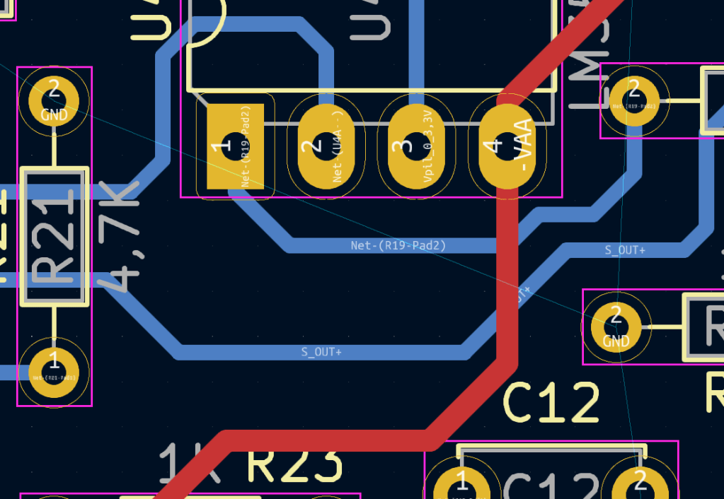
See those two blue traces, one labeled S_OUT+ and one labeled R19-Pad2? When S_OUT+ has a signal running through, it’ll have a voltage. That voltage will polarize the molecules in the dielectric around it, and attract/repel charges in the R19-Pad2 trace, thereby changing its voltage. That’s the definition of a capacitor isn’t it?
At no point in the circuit are they physically connected together by any components, there is no “capital C” capacitor put between them, you won’t find an associated capacitor in the schematic, however they do have capacitance between them. They are conductors with a surface area, they carry charge, and they’re separated by a dielectric — in this case the PCB material (usually FR4, a type of fiberglass). That is a parasitic capacitance.
Crosstalk
Parasitic capacitance exists between *any and every* conductor in a circuit. When a wire or trace has a voltage on it, it induces voltages in surrounding traces through its electric field. This seems obvious when you think about it, and the way we can model this electrodynamic effect is simply with a capacitor. Similarly, when you have currents going through traces, they create magnetic fields which induce currents in surrounding traces, which can be modeled as mutual inductance.
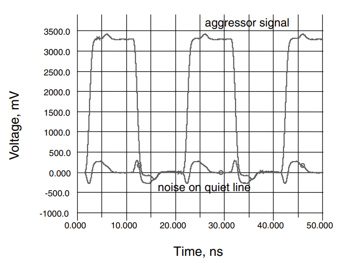
Parasitic capacitance causes all sorts of problems in circuit design that can often be difficult to predict, most notoriously in the form of crosstalk. Crosstalk is the combined effect of parasitic capacitance and mutual inductance. The graph below, from Eric Bogatin’s “Signal and Power Integrity”, shows how a 50MHz square wave affects a nominally 0V line that’s close to it. If the quiet line were a digital signal, this might be okay, but imagine that the quiet line is an analog signal, maybe a pressure sensor. Just being next to a 3.3V square wave causes jumps of over 200mV, that might mean the system accidentally thinking the pressure spiked by thousands of psi! If that analog signal weren’t 0V, that difference could cross a critical threshold and trip the safety system, all because of crosstalk and parasitic capacitance.
Pros and Cons: Semiconductor Capacitors
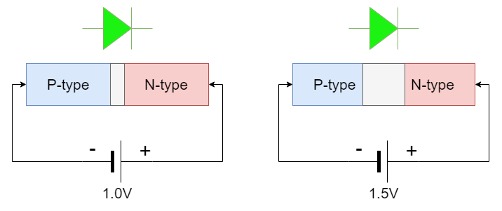
That’s an obviously negative effect of parasitic capacitance, but it shows up in many places and can sometimes be used to our advantage. Semiconductors in particular have capacitances all over the place. A simple pn junction can be a capacitor. When a pn junction is reverse biased, there’s a depletion region in the middle that blocks current flow. That’s two conductors, with different voltages, and an insulator in the middle that prevents charge from one conductor going to the other. In other words: a capacitor. What’s unique about this compared to regular capacitors is that changing the voltage makes the depletion region bigger, which changes the capacitance. That means we have a voltage controlled variable capacitor. The graphic below illustrates this, with the grey region being an exaggerated demonstration of how the depletion region changes size.
BJTs are made up multiple pn junctions, with the base-collector junction usually being reverse biased, giving them an inherent built-in capacitor. This is creates design difficulties and is the subject of much writing.
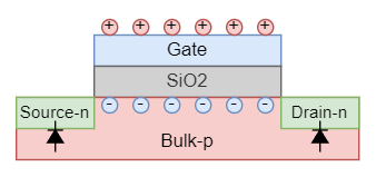
Capacitance in MOSFETs is even more interesting. The very basic operation of a MOSFET involves applying a voltage to a metallic gate, which is separated from a p-type substrate by an insulating layer of silicon-dioxide. It pulls electrons up to the top of the substrate, connecting the n-type source and drain with a conductive path of free electrons. Gate, silicon-dioxide, substrate. Conductor, insulator, conductor. A capacitor. A MOSFET is literally just a capacitor that controls a resistor between two terminals (source and drain). There are other capacitances, such as the pn-junctions between the bulk substrate and the source and drain, as well as between the gate to source and gate to drain. All these can be viewed and used as capacitors.
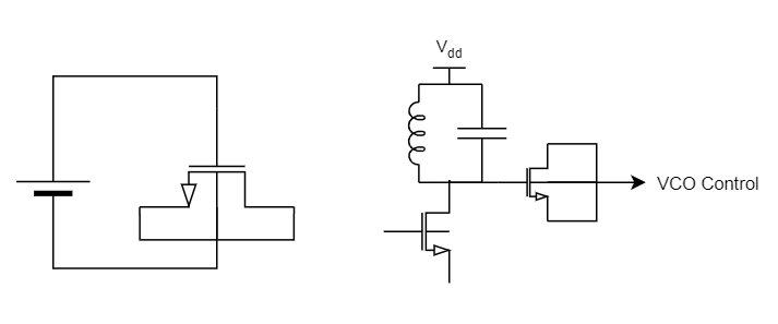
We can actually exploit these parasitics quite successfully. In integrated circuits, capacitors take up a ton of space and can have poor tolerance. By tying the source and drain to the bulk, we turn the MOSFET into a two-terminal capacitor as shown on the left side. It doesn’t have much capacitance, but it’s reliable and controllable. The most prominent application is in a voltage-controlled oscillator (VCO), part of which is on the right. The inductor and capacitor form an LC tank, which naturally oscillates. The MOSFET capacitor is connected to an external control signal that tweaks its capacitance and in doing so changes the oscillation frequency.
So that’s the gist of it. Capacitors are things we can buy off the shelf to put into our circuit, but the phenomenon that capacitors exploit exists in a much more general sense all around every wire and component in our circuits, and that’s what parasitic capacitance is.

One thought on “WTF is parasitic capacitance?”