The world of IC design has this unfortunate chicken-egg problem where you have to have tapeout experience to get a job, but you have to get a job and design a circuit to get a tapeout (tapeout meaning getting your design fabricated). Tapeouts are very expensive, tens of thousands of dollars for a small run using old technology, to possibly millions if using newer state-of-the-art technology. The only way to get this sort of experience is with a PhD, which is hard to get accepted to. It’s one of those “Entry level position, 5 years experience required” situations.
However, over the last couple years, the company Efabless has coordinated a partnership between Google and the Skywater Technologies foundry in Minnesota to open up high-tech IC design and fabrication to the public FOR FREE. That’s right, every single part of this is completely free.
The tools are all free and open source. The PDK, which involves all the design rules and constraints and simulation models for the fabrication devices and technology, which are usually extremely secretive and guarded and requires heavy fees and NDAs, is free and open. And on top of all that, Google is paying out of pocket to fabricate designs for people, meaning you don’t have to pay anything for a tapeout. I’ve decided to try my hand at using this process to design and fabricate something. I’m deciding between a DAC or a programmable switched capacitor filter. We’ll see how it goes.
The first thing to do is to actually install everything. And boy oh boy has that been a process. Through blood, sweat, and tears and weeks of trial and error, I finally got things up and running and began designing and then….my hard drive. With no backups. I couldn’t believe it. So this time instead of installing it on a virtual machine, I decided to use WSL, which is a Linux subsystem that allows you to run Linux applications as if they were natively running on Windows. I re-documented all my steps for you here. This is currently the best way to install all the necessary tools, as of writing this on August 14, 2022. Every other guide and video out there is outdated or misses steps in some form because they’re not starting from scratch. IMPORTANT NOTE that I have not actually used the digital portions of the process (OpenLane/OpenRoad). I have only used Xschem, Ngspice, Xyce, Netgen, Gaw, and Magic to design, simulate, and layout a simple differential pair.
Part 1: Sweeping parameters under the rug
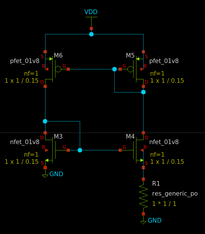
My first task is going to be to generate a good temperature independent voltage source, as well as some circuitry that is stable enough across supply variation and temperature to provide bias voltages for the rest of the circuit.
There’s a couple topologies to work with, but I’m starting simple, partly because of the learning curve on the open-source tools. Everything is a little slower and there’s less documentation and support so it’s a bit of an uphill battle. At 11pm I thought I’d figure out how to calculate the derivative in Xyce real quick and go to bed. I’m now writing this at 3am, and still haven’t figured it out. Maybe I’ll switch back to slow ngspice.
Here’s the topology I’m starting with. The gate of the N and P can go out to N and P channel MOSFETs of different W/L ratios to generate various currents that can generate bias voltages that are good enough. For now.
But first I have to set the widths and lengths of each device. MOSFETs are….a hurricane of complexity, especially down at the nanometer scale. You can’t just guess at values, you’d end up wasting hours upon hours on just two transistors. Thankfully, I went to SCHOOL. I have MATH and BOOKS! MOSFETs are defined by well behaved equations with a few constants, and if we can find those constants we can perfectly calculate the behavior of the circuit. Off in the distance, Lucy sets up a football.
The equations as we know them can be found in the lil cheat sheet I made back when I was studying before grad school. The two main variables to get are un*Cox, and channel length modulation. To do that, we can set up a single transistor with a voltage source at the drain, and at the gate, and then step through them, just like a curve tracer.
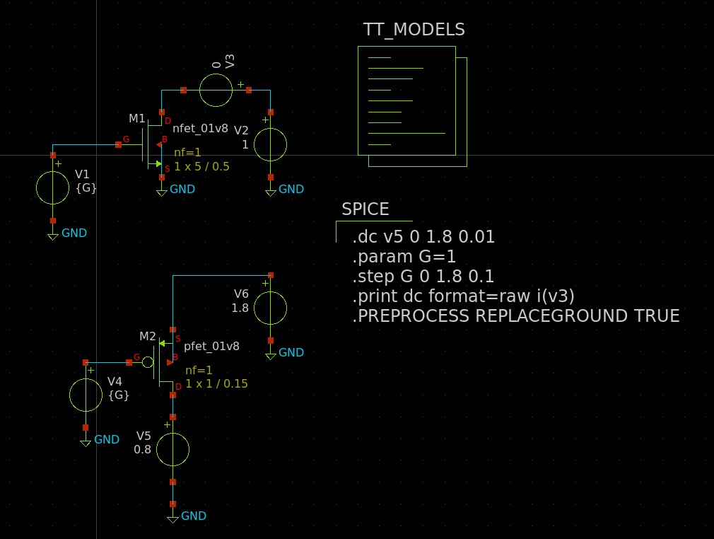
I simulate and get the following curves for the NFET and PFET. I start running towards the football.
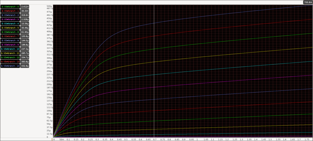
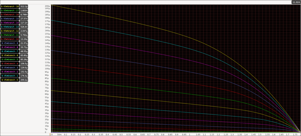
Beautiful. Nice looking curves, about what you’d expect, graphically speaking. There’s a triode region when Vds is low, it’s hits a certain knee bend we can call a saturation point, and then it’s a vaguely straight line because of channel length modulation. With channel lengths as small as 150nm (Yes it’s called Sky-130 but the length is actually 150nm), the exact saturation point isn’t so well defined. It doesn’t just go from inverse square to straight line.
I look at the graph and see the turn on voltage, pick a Vgs curve, eyeball where the saturation point is, and use the current there to calculate un*Cox. Then I go further up the Vgs curve, and find the slope of the line, and use that to find the channel length modulation. I try to kick the football, but Lucy pulls it away, and I go flying and fall on my back.
You see, if I repeat this process for another Vgs curve, I get different values. Raising the Vgs lowers the carrier mobility. If I find the slope at a different Vds, I get different values. If I change the width or length, I get a different threshold voltage! There’s so many axes of freedoms.
But I have a vague framework. For a W/L of 1/0.15, Vth is about 700mV. For a Vgs of 1V, the fabrication specific Kn is about 150uA/V^2, and the channel length modulation is about 0.12 when Vds is 1V. If I increase the W/L ratio, the threshold voltage goes down, but the Kn increases. But then increasing the overdrive voltage lowers the Kn.
It looks like the reality is I’ll need to create a very coarse look-up table, and then create a 5-dimensional tensor in my head like a jackass and draw lines between the points, and then simply re-simulate anytime I want to know more precisely. Awesome. I’m just gonna go ahead and take these parameters and sweep them under the rug.
