4/23/23 – Next up, we have the telescopic cascode op-amp. The point of this is to have a very high bandwidth, not so that it can actually process and amplify high speed signals, but so I can use it for something like an LDO. The cool part about feedback is that it responds to noise and helps counteract it, but it can only counteract the noise that it can sense in the first place. So we need an op-amp that has a very wide bandwidth, a GBW up in the high hundreds of MHz or low GHz, but is responding to very small signals so output swing headroom is not so important.
The reason a wide bandwidth is important is because of how negative feedback reduces noise. When noise goes through a feedback loop, it is first amplified up by each stage, and then loops back around where it’s divided down by each stage. The result looks something like this:
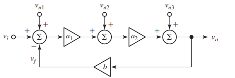
In order for a stage to divide down the noise, it must be able to amplify it in the first place. This is why the pre-amp stage for low-noise circuits like a photodiode detector or scintillator will have a wideband op-amp, not to amplify signals in the 10MHz+ range, but so it can suppress noise in that range.
As a target I’m following some of the specs presented in Razavi’s article on LDO design and seeing if I can match it, but with a different topology. In the article, he says he wants to use a cascode but doesn’t because of the low supply voltage, but in his case the supply voltage is 1.2V while in mine it’s 1.8V. This extra headroom allows me to use a telescopic cascode and achieve high speed with greater flexibility.
I’m not prioritizing low power here, which means I can drive the bias current up as needed to 300uA+. This is good because it lets me get higher gain without having to make the transistors too large. Large transistors means greater parasitic capacitances and lower frequency poles in the signal path. It does come at the cost of worse flicker noise performance. I have no idea if that will really matter for this. I’m going to use a simple single transistor current mirror for the tail current because we don’t want to constraint the voltage headroom *too* much, but I may later opt to create a current mirror with great output resistance to improve CMRR.
What I learned from the last op-amp is to just set the lengths to all be the same and be done with it. For high speed in my 65nm process, I’m going to set the lengths for everything to 90nm. Running a simulation of this, the channel length resistance rds is high enough to get good gain with cascoding. But then what I’m finding is that for a given W/L and Id, the rds changes depending on the overdrive voltage. This is because I have the source of my test transistor tied to ground, which it won’t be in practice, and this is messing up my test bench. I put a current source above and below so the transistor is floating and I can get a more accurate value, and with a W/L of __, I get an rds of ___ and gm of about ___ . This is not bad! Even the Vdsat is below ___, which should result in a voltage swing headroom that’s more than adequate (if I get more than ___ swing I’m happy).
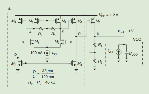
N.B: – The PDK I’m using is an actual one, TSMC’s 65nm process. In school you use something like “gpdk180” which is a purely educational one. My RFIC project partner is doing a PhD and we did a VCO in advance of his thesis, so we got this PDK and I signed an NDA, which means I can’t divulge any information specific to it. Anything actually showing numbers like gm/Id or threshold voltage or body effect or parasitic capacitances are protected info. I can show schematics and results but no process information.
What’s interesting in these component tests is that while lowering the bias current of course decreases the gm, the output resistance proportionally increases. In a cascode configuration, the output resistances get multiplied, while the gm of only one device dominates the gm of the whole amplifier. So I could potentially reduce the tail current for the pair from 300uA to 200uA and actually *improve* the system.
I take note of this and then smash together the telescopic OTA, or at least its skeleton. I’m going to start off by using ideal sources for all the biasing, but I think I’d be cheating if I just used that for the final design and called it a day.
4/30/23 – My photonics final is over, time to relax. I’m gonna work on this project but I feel like before I can tackle this, I need to really get a better handle on current mirrors and biasing. Detour time! Also I’m unsatisfied with the way I’m designing things, I’m already relying too much on bad habits and fake rules of thumb, I need to learn a better way to size transistors like gm/Id or inverse coefficient or whatever. Detour detour time!
5/7/23 – Lazy Sunday so I spent the day learning a bit more about gm/Id and how to size transistors. I have to say, I’m quite a fan of this. I’m using hand calculations for some parameters, then sweeping a device under different conditions to create graphs and using those graphs to get other parameters and finally device sizes.
Setting up testbenches to get these graphs is a pain though. Cadence has Ocean scripts and they’re not terribly intuitive.
5/9/23 – I’ve done out my hand calculations and, using the various graphs I’ve created I’ve got a starting width and length for the different devices. I’m targeting a gain of 50dB and GBW of 1GHz. This should be achievable if I get a gm of 1.5mS for the input transistors, 800uS for the other transistors, and an rds greater than 10k for input transistors and 25k for the rest.
What I really like about it is that it feels more like how design should be, it lets me start with my results and work backwards from there. The actual resulting length and width is only incidental, a consequence of the combination of performance metrics I’m trying to hit.
Before I test this out, I need to bias all the transistors. This is no small task, I don’t want to simply pick a voltage that’s within a window that will keep each device in saturation. Better to properly have the biases set by current mirrors. It’s like Baker says “the three most important things in analog design are biasing, biasing, and biasing.”
5/14/23 – Today I’m working on the biasing circuits. I connect to the VPN and remote Linux server and then realize I forgot my credit card at the bar last night and do a miserable walk-of-shame to get my life in order. Anyways. With the 5-transistor OTA, I didn’t focus too much on biasing and I just used an ideal voltage source for each transistor. Not only that, but I used an ideal voltage source shared between the two branches of the diff amp. In reality, the two transistors will have different threshold voltages, so even if everything else were perfectly matched, using the same bias voltage would result in an imbalanced amplifier and it would pretty much immediately saturate.
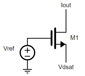
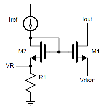
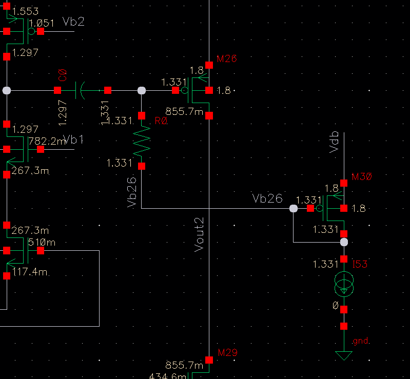
Reading through Baker’s CMOS book, he goes into quite a bit of detail on a Beta-Multiplier Reference circuit which can be used to generate biases for a variety of circuits and situations. I’m studying up on it but in the meantime I need to just get this core telescopic OTA working in the first place. What I’m going to do is set up biasing for each transistor as a current mirror, but I need to take care that both transistors are floating in a similar way and staying in saturation. My plan is to use the scheme below. I think if I keep VR roughly similar to Vdsat, it should be okay. With this simple current mirror setup, the concern is the output current changing with varying Vds, but in the telescopic op-amp that will be a fairly restricted range. At least that’s my thinking.
This doesn’t need to be actually *good* biasing, it just needs to work well enough for simulations with ideal components so that I don’t have to worry about it here. In the future I will likely come back to biasing and spend a lot more time on it. From what I’ve seen in my simulations, each transistor *roughly* has a saturation voltage of a couple hundred millivolts. I set the resistor based on that for each transistor. While normally I would set the transistor such that I can keep Iref small and save power, I’m not concerned with that here.
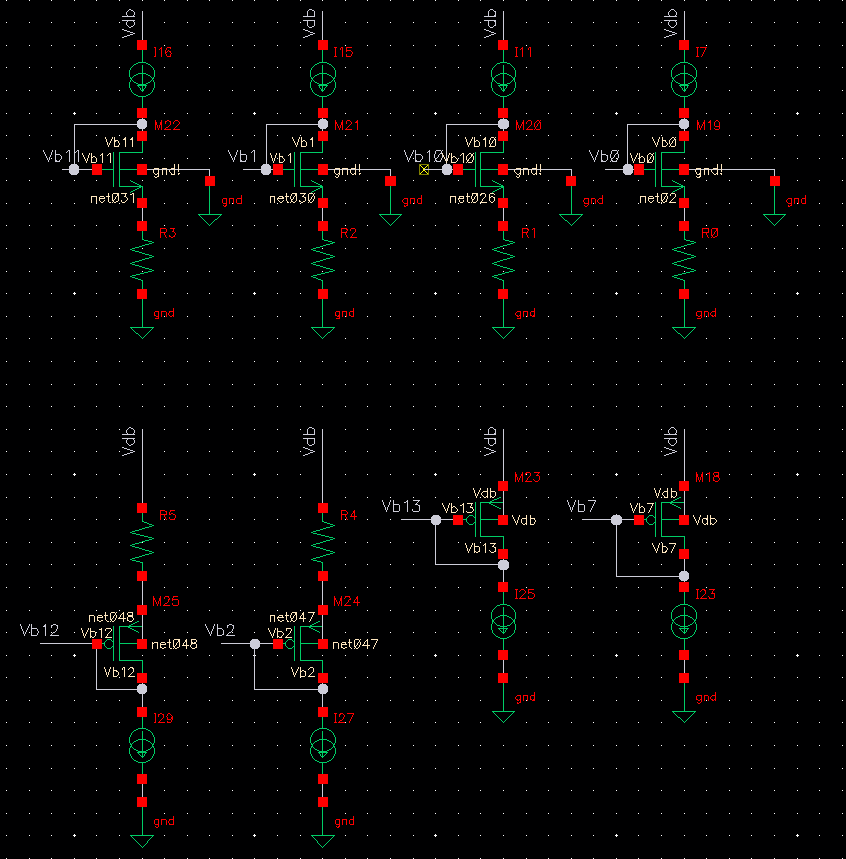
I drew up the biasing circuit. I have no idea how or if it will work. What’s scary to me every time at these points is that I might only have one single small number off, but if one small thing is off the whole thing breaks which makes it look like every part of this machine is broken. It’s right about time for the new Succession, so rather than risking a bad simulation now, I’m just gonna stave it off for later.
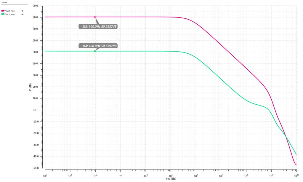
5/16/23 – I run my simulations with my hands over my eyes. Based on my hand calculations and using gm/Id plots, I actually got very close to what I wanted on a first pass! On my input transistors I was shooting for a gm of 1.5mS, and I got 1.48mS, I wanted an rds of at least 10k, I got 11.9k. For the cascode NMOS I wanted a gm of 800uS and rds of 25k, I got a gm of 980uS and rds of 24.8k. For the PMOS though it’s not quite what I expected, but then again I didn’t actually do anything to really size them and just assumed widths of 2.5 times that of the NMOS.
Looking at the open loop gain, a 100uVpp input yields me an output of 41mVpp, which is a gain of….52dB!! Incredible, I was targeting a gain of 50dB and I’ve got it! It probably isn’t stable but we’ll worry about compensation later. For today I’m happy. Next up is designing the CS stage. Because my telescopic first stage has such high gain, I only need a gain of 10-20dB or so on the CS stage, but I need fast response and wide swing.
5/21/23 – I designed the CS stage today. This part was harder than I expected. What always trips me up is getting the common-mode voltage correctly. At some point I’ll need to properly design a common-mode feedback circuit. Today is not that day. I changed the OTA to a single ended version, which helped.
Secondly, I was doing something stupid which is that I was using a current mirror to bias the input transistors, and then capacitively coupling in the input signal. This was giving me weird results and I went down a rabbit hole for like an hour trying to figure out why my op-amp suddenly turned into a crappy bandpass filter. The current-mirror biasing was still useful though, I just biased the input with a DC voltage source with the voltage output by the current mirror, and that pretty much instantly fixed my issues.
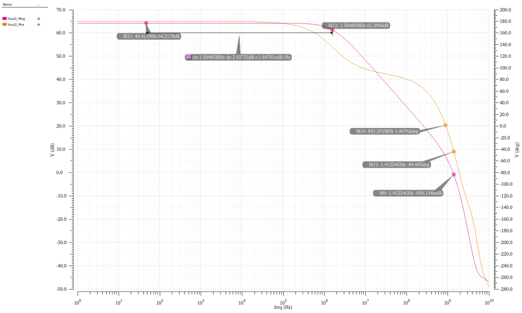
These are promising results. I designed for a gain crossover of above 1GHz, and got one of 1.4GHz. I wanted the second stage to have a gain of 15dB, if the total gain is 64dB and the first stage is roughly 52dB, that’s a gain of 12dB. I would’ve like maybe a bit more but for a 1.4GHz GBW op-amp, 64dB open-loop gain is phenomenal. You can also see how it’s a perfect -20dB/decade slope from 1.6MHz to 1.4GHz. I love that.
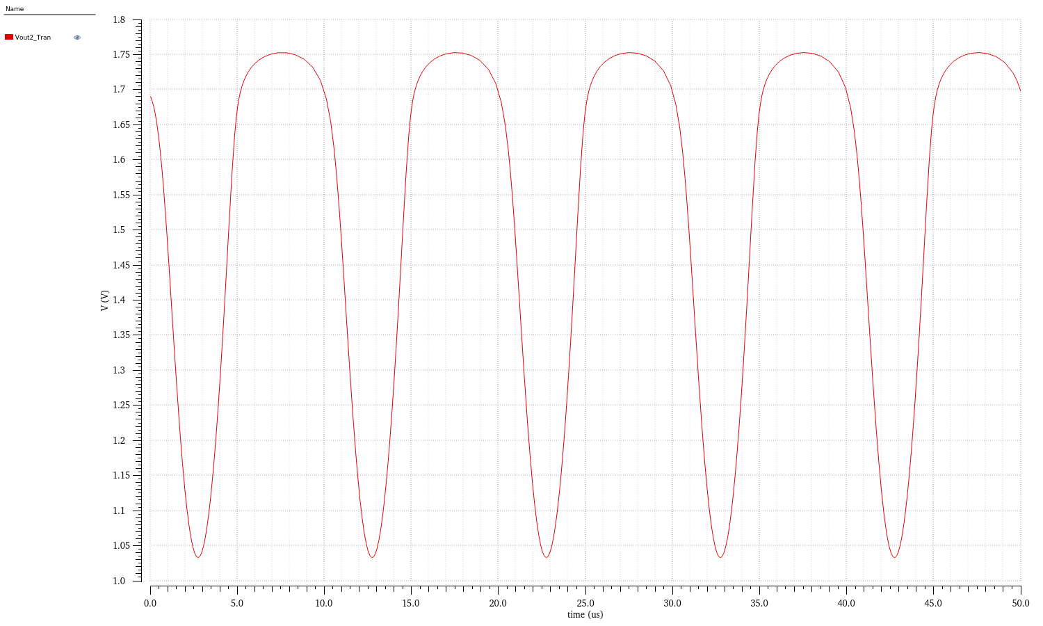
5/24/23 – The output transient is horrible though because the two stages are directly coupled, so the output DC is way up at 1.6V, leaving little to no headroom at the top. To fix this I bias the CS stage and capacitively couple in the output of the first stage like so. The screenshots below show the transient output without biasing, the transient output with biasing, and the biasing circuit.

What’s interesting with this though is that when I look at the operating conditions of the CS stage, it has a gm of 2.4mS and an rds of 26kOhms, which should give me a gain of 35dB. If that’s so, shouldn’t the gain of the whole thing be more like 80 something dB? Indeed when I plot the output of the first stage, it’s been degraded by the biasing. The gain of the first stage is actually dependent on the value of the resistor used by the biasing circuit. If I increase the resistor from 10kOhm to 1.0MOhm, the gain of the first stage goes back up to ~51dB, and the second stage is 30dB, with the overall gain being above 80dB. That’s a spicy meatball!
There’s a section in Razavi’s CMOS book that has some good info about biasing that has a few suggestions and improvements that I may try out later. The DC and AC characteristics look great, but the stability is atrocious, pretty much non-existent. For some situations this doesn’t matter (and I have basically 0 ability to judge which situations those are), but since I’m more or less building this to control an LDO, open loop stability is a must here. I think. Or not. Somebody please tell me.
5/31/2023 – Spent the weekend going heavy into gm/Id. Now I’m ready to finish off this op-amp by compensating it to achieve stability. Phase crossover at 350Mhz, and a phase margin of 60 degrees is achieved at 100MHz. If I move the dominant pole down to under 4 decades below that — 10kHz or so — that would do it.
In a 2-stage op-amp, the formula for the new frequency is:
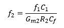
where C1 is the load capacitance of Stage 1, Gm2 is the transconductance of Stage 2, R2 is the output resistance of Stage 2, and Cf is the feedback Miller capacitor. I now have a phase margin of 53 degrees, which is almost exactly the same as the one in Razavi’s LDO, so I think we’re good!

I know my plan was to do a thorough testing and characterization, and then improving an aspect, but this one has been dragged out so long. Life got in the way, and I stopped to learn gm/Id stuff which I spent a significant portion of time on, and I started doing some biasing tests. So I’m just gonna move on to another building block, which is a biasing system like the Beta Multiplier Reference. After that, plus having the gm/Id setup, I’ll get back to properly tackling op-amps.
