My goal is to put all the critical info needed to successfully do simple designs in one place, both for my reference and to give others a starting point. I have found no start-to-finish resources explicitly laying out how to do it, this is stitched together from reading the books and a dozen different Cadence threads with people saying “I can’t figure this out edit: never mind got it!” and refusing to elaborate further, or Andrew Becket (PBUH) solving a super specific problem that’s tangentially related.
This is not a substitute for doing the reading and going through these concepts yourself. Please do not ask me to troubleshoot your designs (I’ve gotten literally dozens of emails and messages asking me for tech support on the Sky130 install instructions I posted, please don’t do that). If, however, you have suggestions or corrections or constructive feedback, please reach out.
GitHub repo with relevant scripts can be found here. These scripts are being updated as I use them, right now they’re fairly rudimentary to get up and running.
1: The gm/Id Methodology
a. Background
Analog design is hard enough as it is on paper, doing analysis and coming up with topologies and trying new ideas, but a lot of time is wasted on getting the size of the transistor. I have given specs and bandwidth and noise and gain, maybe soft limits for power and area, I can figure out things like gm and rds from there, why am I twiddling around over width and length? Because that’s the only thing I physically have control over.
The gm/Id methodology allows you to focus on the actual design, and then use numerical simulations to match those design specs to corresponding widths and lengths. That way I can quickly try out various topologies and not be a SPICE monkey.
The two main books on this are Systematic Design of Analog CMOS Circuits by Jespers & Murmann, and Tradeoffs and Optimization in Analog CMOS Design by David Binkley. Both are conceptually built off the EKV model, which aims to have one unified analytic expression across all regions of operation for submicron transistors as opposed to the square law which has been fairly inaccurate for a few decades now.
b. Equations
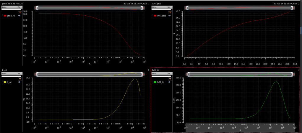
Let’s lay out all the important equations as they relate to the Intrinsic Gain Stage (meaning a CS stage with ideal current source load driving a load capacitance) right here, all in one place:
Equation set (1) is related to the “large signal” form of the EKV model and its inversion coefficient. Equation set (2) describes DC characteristics. Equation set (3) describes AC characteristics. Equation set (4) are figures of merit.
Most of these variables should be familiar to anyone who’s taken an intro analog IC class but there are some new ones. “n” is call the subthreshold slope. In subthreshold operation, the MOSFET’s I-V curve is exponential, which when graphed on a log scale looks linear. The slope of that linear log scale graph is n. n is process-dependent but typically between 1 and 1.5. Phi-t is thermal voltage, roughly 26mV at room temperature.
There are multiple angular frequencies in equation set 3. wc is the 3dB cut-off frequency (GBW/Av), wu is the unity gain frequency a.k.a. GBW, and wT is the transition frequency when the device itself can no longer achieve any gain due to parasitic capacitances. FO is the fan-out, the ratio between the input and output capacitances. This is very important in digital design as it determines propagation delay, but it can also provide insight in analog design for stage loading. In general, a design with a fan-out below 10 is a bad and unpredictable design.
c. Methodology
The steps to the methodology vary depending on what’s given as a spec and what’s being optimized. For example, we may have a hard-set power/current requirement, or be area constrained, and now it’s everything else we need to find. An example may be the following sequence
- Load capacitance and bandwidth are given, therefore gm has a hard spec to meet.
- We choose a length (or range of appropriate) lengths based on application. Shorter lengths optimize speed, large lengths optimize gain.
- Choose an inversion coefficient. 0.1 is weak inversion and optimizes noise and power, 10+ moves into strong inversion and optimizes speed and area, 1 is moderate inversion and is a good starting point compromise.
- Calculate gm/Id from the inversion coefficient, then Id.
- Use the LUT to graph gm/Id vs Id/W. Calculate W to get a W/L.
- Use the LUT to find the resulting FO and confirm it’s at least 10 if not much greater.
That’s it. It’s of course an iterative process like all circuit design, maybe you’ve designed most of the other circuit and now this one transistor has to have dimensions and specs it physically can’t meet so you’re back to the drawing board, but you can focus more on topologies, impedances, specs, PVT issues, and less on simply “What’s the W/L?”
The LUT is of course the Look-Up Table. Rather than repeatedly running parametric sweeps for various situations as you come across them, you write a script to run every simulation you’ll ever need for each device in a process, and then use a Python script to quickly extract and graph any info. Ideally, you can do 90% of your design process on paper and in Python, without ever touching Cadence. Then when you go to Cadence for schematic entry and verification, the design should match quite closely on the first try, and then you can tweak from there.
While the gm/Id methodology is simple and elegant, generation of the LUT is a pain, and takes a long time and needs to be set up and run for potentially hours per device to get enough resolution. The next 3 sections cover LUT generation and usage, with the repo above available for reference. I’m partially recording all this here for my own benefit, but I also hope it saves other people time.
2: Setting Up The Schematic and ADE Simulation
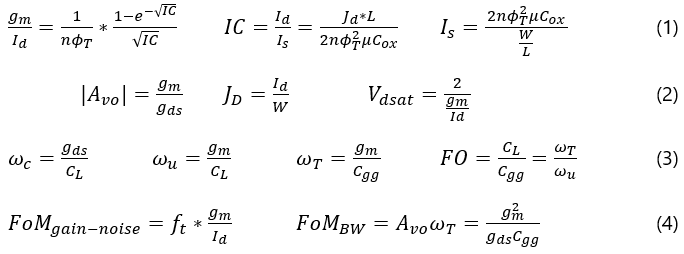
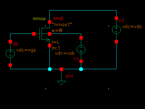
First, set up the schematic to look like the schematic below. You may also choose to add a current source and use that for one of your sweeps, in which case you’ll need to calculate the upper and lower bounds to not go over your device’s current density limit. I’m using the setup shown here to replicate what’s shown in the textbook.
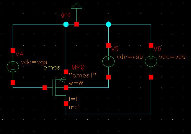
Then set up the sims to look like the following, except do it in ADE L. Setting it up in ADE L makes the scripting much simpler. If I have time I’ll try to provide a script for Maestro. The “waveVsWave” functions are just to confirm your setup works, we’ll delete them later in the script.
For a given technology — I’m using gpdk180 here — it should provide plots that look like the following. This is for one given length, with VDS and VSB held constant.
Save it as an OCEAN script (Session -> Save Ocean Script) in ADE L. We will modify it to iterate through several lengths, VDS, and VBS loops and run this sweep each time to effectively give us a 4-D table. Width doesn’t actually matter, every parameter scales quite linearly with it, which is why we’ve captured it in the current density figure Jd = Id/W. The Jespers/Murmann book sets width to a constant 10um, you can also set a constant W/L ratio like 20/1. This guide follows the book and uses a constant 10um width.
The OCEAN script will save every single point as a line in a CSV with all relevant info. Setting it up is a bit annoying (or you can simply copy my script and tweak it), and then running takes a long time depending on how many permutations you want, but this process only needs to be done once per device. After that, we can then extract this info with a Python script, and write functions to visualize the data and design graphically.
3: Edit the OCEAN Script (or download from github and skip this)
The original OCEAN script output from my simulation can be found in the git repo. The beginning section is going to differ installation to installation, you’ll have to use whatever is specific to you. I wrote and tested this on my school’s servers where we have limited home folder space but virtually infinite space in the /tmp folder, so my netlist and resultsDir are under the /tmp folder. My setup at work is quite different so I’ll need to edit accordingly.
The modified gm/Id OCEAN script is in the repo as well, “gmid_ocnade.ocn”. It is commented, but I will run through the edits I made section by section and explain it out. Do not simply copy and paste the script. I’ve written it for my file system and how I like it organized. Instead read through my rundown and comments, and apply the same edits to your OCEAN script. First duplicate the original so you have a backup.
a. Clean up the analysis
Remove the outputs. That means all the “plot” and “waveVsWave” stuff at the end of the script. We’re going to instead output everything to a file using the “ocnPrint” function.
ocnPrint( ?output outputfile ?numberNotation 'engineering ?numSpaces 10 length_wave gm Id gds cgg vgs vds vsb gmId Jd ft Avo FoM)Function arguments are specified by the ? string and then the value comes after, so the ?numSpaces argument is for the number of spaces between each printed wave, and 10 sets the numSpaces argument. After that, we enter all the waves we’d like to output.
There is a bit of an annoying thing here, which is that ocnPrint can only be used to print waveforms, and the length is a constant variable. To turn any variable into a waveform, I defined a procedure
procedure(
	vartowave(var refwave)
		varwave0 = ((refwave+1) * var)
		varwave1 = (varwave0 / (refwave+1))
		varwave1 ;return variable as a wave with length of refwave
)
and then call it just before ocnPrint.
length_wave = vartowave(VAR("L") vgs)The code above creates a user-defined procedure called “vartowave”. Take careful note of the parentheses. The procedure multiplies a wave “refwave” by a variable “var”, and then divides it by the wave, leaving behind a waveform that is the length of refwave but every element has the value var. The +1 is there to avoid dividing by zero. In this instance we’ve taken the transistor length variable L and turned it into a wave the size of VGS (which is what’s being swept in the DC analysis so every parameter of interest will be an array of this length).
b. Create a procedure
We want to take the DC sweep and turn it into a procedure that we can adjust and call over and over. I create a procedure to wrap around everything from “analysis” down to the “ocnPrint” we wrote earlier. Again, note the parantheses.
procedure(
	simsweep(outputfile length_in vbs_in vds_in)
		analysis
		.........
		ocnPrint
)
We will call simsweep in some for loops, and that will do the bulk of the work. You also want to go in and edit the analysis to actually use the argument variables. For example, the ADE variable L is tied to the OCEAN variable length in the analysis simsweep procedure with the line
desVar( "L" length_in )Do this for all relevant variables.
c. Iterate through loops
Now we create the variable sweeps we iterate through, and the for loops that iterate through them. First we create an empty CSV file for everything to go into.
resultscsv = outfile( "./nfet_gmid.csv" "w")
close(resultscsv)
Then we setup the lists of variables. For simplicity and to test if your code works okay, keep it small before doing the higher resolution sims.
len_list = list( 180e-9 500e-9 )
vbs_list = list( 0 )
vds_list = list( 400e-3 700e-3 )
Then we create the for loops that contain the simsweep procedure we created earlier.
for( k 1 length(vsb_list)
	for( j 1 length(len_list)
		for( q 1 length(vds_list)
			tempout = outfile( "./adel_out.out" "w")
			simsweep(tempout nthelem(j len_list) nthelem(k vsb_list) nthelem(q vds_list)) ;simulation run and saved to temporary output file
			close(tempout)
		)
	)
)
Inside the lowest level sweep, Vds, is where I put the simsweep function, and I create a temporary output file adel_out.out just for that one sweep. That will be appended to our resultscsv from before.
d. Output to CSV
SKILL has a “system” command which allows you to use UNIX shell commands from Cadence. We’re going to use that to basically do file concatenation through bash commands to create our consolidated look-up-table. Put this in the lowest foreach loop, right after close(tempout). NOTE: This is really finnicky, I’ve found it works differently on different setups, so you may need to edit this on your setup. I’ve left in commented-out lines of code (semicolons are comments) that were necessary in one setup but not another.
;system(sprintf(nil "sed -i '2 r ./nfet_gmid.csv' adel_out.out")) ;existing CSV inserted into output file below header
system(sprintf(nil "sed -i '/^[[:space:]]*$/d' adel_out.out")) ;empty lines deleted
;system(sprintf(nil "sed -i '1d' adel_out.out")) ;header deleted
;system(sprintf(nil "rm -rf ./nfet_gmid.csv")) ;old CSV deleted
;system(sprintf(nil "mv ./adel_out.out ./nfet_gmid.csv")) ;new output file renamed as CSV
system(sprintf(nil "sed -i -e '1d' adel_out.out"))
system(sprintf(nil "cat adel_out.out >> nfet_gmid.csv"))
;system(sprintf(nil "rm -rf ./adel_out.out"))
And that’s it, we’re done! The script overall defines a simulation, sets up variables to iterate through, runs the simulation through a for loop, and outputs all the data to a CSV file to be read and interpreted from Python and MATLAB.
Once you’re happy, go to the Virtuoso window and enter the load() command to run the script.
4: Extract the Info in Python
Note: this script is still in progress so this text may be out of date.
Getting all this data is completely pointless if we can’t sift through it and extract the info we need. I created a Python script with functions to get exact values, and to graph curves. Both are needed to give insight into the device and process. Copy the CSV file created earlier to a local directory and clean it up, and name it after the device the data is taken from.
We load the CSV using Pandas and filter through it by length, VDS, and VSB. The Jespers/Murmann scripts are able to do interpolation. As of the posted date, I have implemented a fairly rudimentary interpolation method, use at your own risk.
Pandas makes it simple to integrate Excel-like filtering functionality without having to touch that god-awful interface. All primary functionality can be found in the gmid_test Jupyter notebook, but I’ll show a snippet here.
from paramExtract import gmidLUT
import matplotlib.pyplot as mp
nfet = gmidLUT('nfet_gmid.csv', 'nfet')

vsb = 500e-3
vds = 700e-3
L = [500e-9, 1e-6, 2e-6]
nfet.plot_jd(vsb, vds, L)
nfet.waveVsWave(['vsb', vsb, 'vds', vds, 'L', L], 'jd', 'gmid')
The CSV is named “nfet_gmid.csv”, so we instantiate it with gmidLUT(‘nfet’). We provide the Vsb, pick a Vds, provide some lengths, and we can plot the Jd vs gm/Id curve either directly with the plot_jd command, or manually with the waveVsWave command. If you want to do other processing, like interpolation, you can pull the data into an array using the wavefilterNP command, seen in the Jupyter notebook.
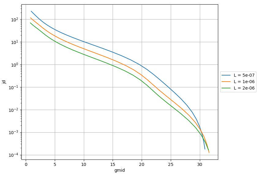
If I need a gm of 100uS, and I can only consume 10uA, that gives me a gm/Id of 10. For the 500nm transistor, that corresponds to a Jd = Id/W of 10. That means the W must be 1um, so my transistor is 1um/500nm. No guessing or repeated simulations needed, I can get all this info quickly through Python natively on my own computer rather than fumbling through parametric sweeps on Cadence on a remote desktop every time I need a number, and it’s guaranteed to work on the first shot.
