6/5/2023 – This is the first time I’ve designed a fully differential amplifier. I was planning on the telescopic being differential, but I was having so much trouble with it since I was learning how to properly do parametric sweeps, and how to bias. Small steps.
The reason I’m creating this single stage OTA is to 1) keep it simple and focus on the CMFB and 2) I’ll need it later for either switched-capacitor amplifiers or Gm-C filters.
Single Ended
6/6/2023 – I did some calculations, and sweeps, and put together this amplifier. Unlike my previous ones, I’m going a bit more on the lower feature size (don’t put that on your dating profile), so the gain I could achieve is lower because the output resistance is closer to just 10k or so.
And look! Look! I’m using the BMR I made earlier! And it works great!! I’m so happy, I can just throw in blocks that I made myself. Amazing.

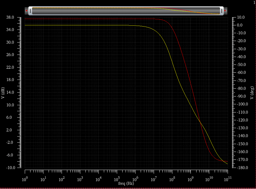
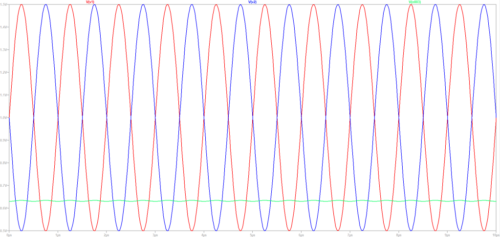
Crazy wideband already, 100MHz 3dB point with 4GHz gain crossover which….look I know that’s not a lot for all y’all IC designers, but coming from PCB design where anything above 10MHz GBW is considered pro, this is fun to see. Plus it matches what Razavi was getting in that LDO op-amp from my last post, because that was a fully differential OTA! Again, there is nothing I love more than when theory is reflected in practice.
Differential
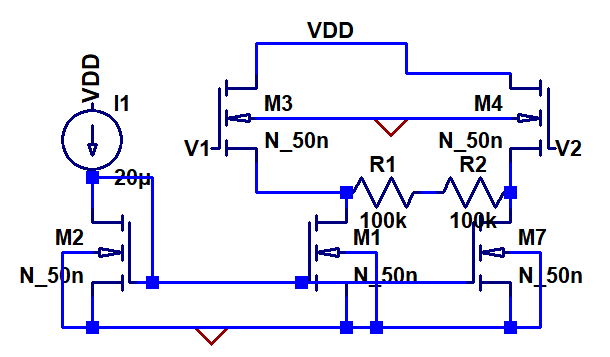
6/7/2023 – Okay now time to make this differential, and create a common-mode feedback circuit. The two PMOS loads are not a current mirror of the tail current anymore, they are now the current sources that bias the amplifier. Our kids are growing up :’)
6/10/2023 – I create the current mirror setup to get ~160uA in each branch, like I had with the single-ended version. I set up a common-mode sensor, by buffering the outputs with a VCVS, and getting the midpoint. This lets me simulate without loading the output and getting the exact common-mode. This then goes to another VCVS which acts as an ideal amplifier. Using a VCVS made it difficult for the simulation to converge since it’s driving a capacitive load, so I switched it to a VCCS.

After much finagling and trial and error, I found something interesting, which is that it works better if the gain is lower, something between 10 and 100, but generally l found keeping it close to 10 provided the best results. I’ll need to come back to this analytically to understand why.
7/15/2023 – It’s been a crazy month with a lot happening in my personal life, but I’m back finally.
I’ve decided I’m going to try something else. Put my brains to use here. I’ve been doing a bit *too* much reliance on numerical methods and copying topologies from references, while neglecting to do proper small signal hand analysis and actually thinking about the amplifier design and feedback loop. First off, rather than controlling the tail current, I’m going to set the tail current with a current mirror like normal and then control the gate of the PMOS loads instead.
Here’s how I’m coming up with a topology. I figure that in a differential amplifier, the node they share between them stays at a common DC voltage. Maybe I can do something with that here.
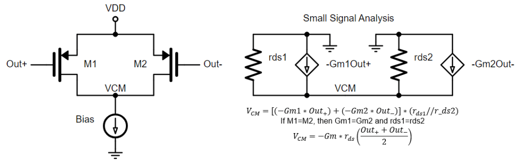
This tells me that if I make Gm*rds equal to 1, the output at the VCM node will be the average of the two outputs from the differential amplifier. Good to know. Also important to know that the polarity doesn’t matter.
Next step is to take that common mode voltage and compare it to something, a current or voltage. I know what I want the common mode to actually be, I can just create an error amplifier. Note the polarity here. If VCM goes up, it’s because the active loads of the original amplifier are being pulled into triode mode because the Vsg is too great, which means their gate voltage is low and needs to go up, and in this case Vout will go up and put the PMOSes back in saturation and stabilize the drain voltages per Vref.
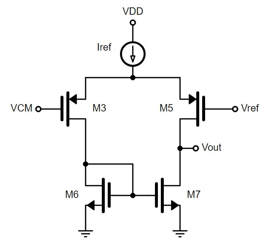
Putting it all together, this is what the op-amp looks like. Interesting how many more transistors there are to create a fully differential amplifier, even a single stage. Looking at the feedback loop, I now understand why some texts recommend the error amp should simply be a gain of 1. The error is being converted to a current by M8, the tail source, and that current is being converted back to a voltage by M11 and M12. The equation is being directly reversed. These should be equal and opposite. So unity gain it is, which is nice because that means we can use smaller transistors, so even though the CMFB has more devices they should be a small footprint overall.
7/24/2023 – Alright let’s get to designing. Unity open-loop gain means small gm and rds, so let’s go straight to minimum length, and sweep widths for different biases. I can just grab the intrinsic gain directly, since that’s what’s in the equation. I find that a bias current of 100uA and a W/L of 2 (two!) gets me a gm*rds of right around 1. Of course this is assuming that M13 has a large output resistance.
For the second amplifier, it’ll be a fairly similar thing, only this time it’s a whole OTA, so it has a load and everything. This time rather than being the intrinsic gain I have to do some algebra. Uggghhh. The resistances are in parallel, so if I want the same overall gain I could get double the intrinsic gain for the NMOS, and then design the PMOS for the same resistance to halve it. I want to keep size and power low, so I stick with an W/L of 2 for minimum length and size and bias current of 60u. Remember we want to make the impact on the physical dimensions and such minimal for this. It gives me an intrinsic gain of 2.3, so that combined with the load and other parasitics should give roughly unity gain.
From what I saw in the simulations, it’s good to overshoot by a little bit, which I can do by using even less power, so I’ll go for that.
And at 1:30am…..I just realized that I did all my parameter sweep flipped around. I’m too sleepy for this right now.
7/25/2023 – The new bias current for the CM sense is 60uA, and for the feedback OTA it’s 40uA. At 40uA, the output resistance of the PMOS is about 33k, so that’s what we want the NMOS load to be, which gets us a W/L of 2.5u/100n.
Aaaaand it failed. Completely. It just immediately went to 1.8V which sent the PMOSes into deep triode and no sensing happened so the amplifier swung to ground and turned off the whole amplifier. I’ve tried a few combinations and permutations and I realize this is not actually sensing the common mode voltage. It senses the small signal common mode, but not the actual voltage. Looking at it, and then going back to read some material, I see that the CM sensing techniques are all trying to maintain large signal levels, and then it’s the feedback amplifier where we worry about other stuff.
One of the suggestions is to use source followers on the output, which I do immediately see the drawback of, but testing it out in LTSpice it works. I kind of just want to get this amplifier done with lol.
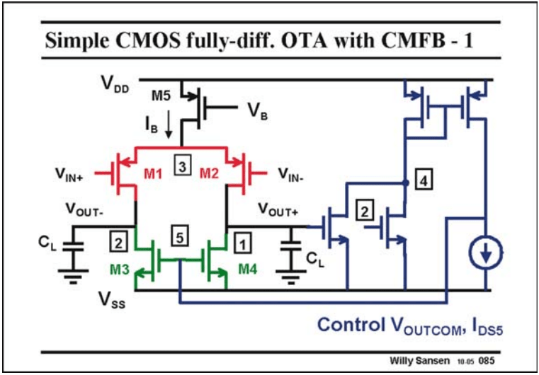
7/27/2023 – I made a post on reddit about op-amps and when I talked about how much trouble I’m having with CMFB, and an experienced designer said “CMFB might be the hardest common circuit to design”. I now see why. So considering how long this is taking me and keeping me from trying out other circuits, I’m going to give this one final shot today and if it doesn’t work out I’ll move on. But then again, Sansen says that while fully-differentials with CMFB are tough to deal with and take up additional space and current, all mixed-signal design must by definition be fully differential the whole chain. I guess I better get used to these.
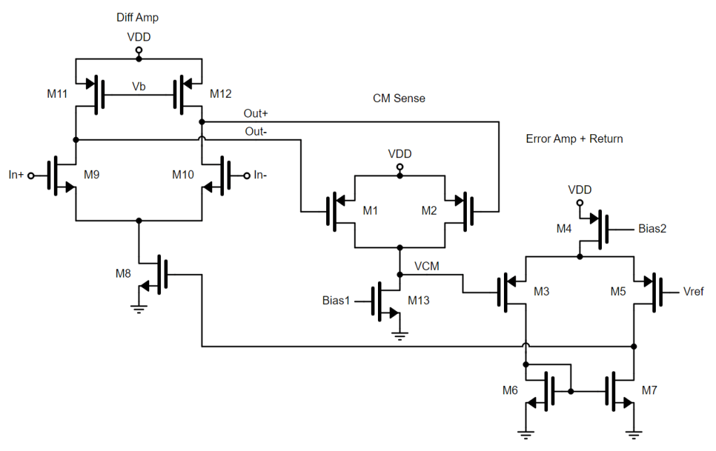
I went back to the circuit I had originally been trying, but read Sansen’s section on it. I noticed he had something similar to what I was doing, but took the output of the sense circuit and turned it into a current mirror.
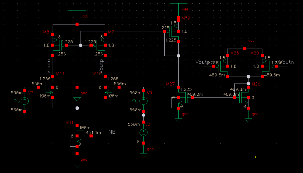
Here’s my circuit
Fingers crossed aaand…..I DID IT!!! IT WORKED!!! Beautiful look at that.
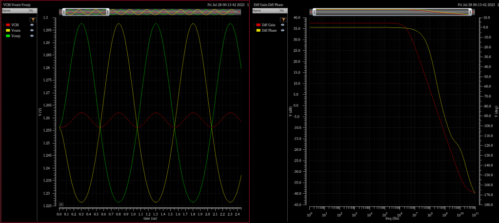
A few notes here, the CM still has some ripple, it’s not held perfectly stable, and the GBW did in fact decrease, I may have accidentally added a dominant pole in here somewhere. I’ll need to play with some parameters from here but honestly I’m just happy to finally get it working right as I was about to give up.
Anyways tomorrow is my last day at my current job, so now that I’m happy I can get some rest, put in one last day, and then spend a week relaxing and….probably trying to make an LDO before my new job.
