6/1/2023 – Gonna be honest, the telescopic cascode was kicking my ass. The biasing was insane, and it was such a time consuming process. So what I’d like to do is spend time on the “support” circuits that help oil the gears of the machine.
Theory
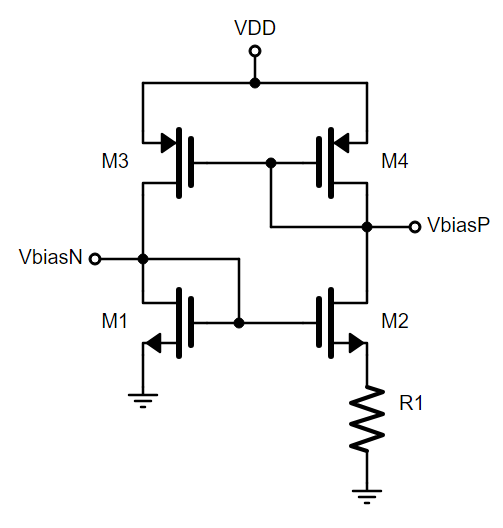
The circuit below is the core of the beta multiplier. Usually we associate “beta” with BJTs, but some texts use beta to denote the 1/2*un*Cox*W/L part of the square-law equation.
The core part is the circuit below. By KCL, M1 and M3 have the same current. But M4 and M3 are a current mirror, so M3 has the same current as M4, and thus M1. Then by KCL, M2 has the same current as M4. And finally as a current mirror, M1 has the same current as M2.
VbiasN is a diode-connected voltage above GND, and VbiasP is a diode-connected voltage below VDD. They all lock each other in place, the left and right branches have the same currents — so long as they are sized such that they are in saturation (this is key). M1 and M2 have the same gate by definition, and because there’s *some* current going through R1, M2 necessarily always must have a lower Vgs than M1. If the current through them is the same, then the beta and thus W/L for M2 must be larger than M1 to keep it in saturation. Take a look at the MOSFET equation again. So we size R1 and make M2’s W/L a multiple of M1’s, one beta is a multiple of the other. Beta multiplier.
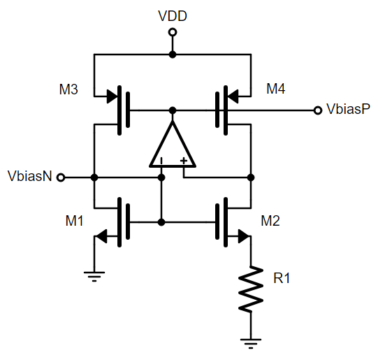
As we know with current mirrors, M1’s gate and drain is the same and theoretically therefore M2’s gate and drain should be the same. M2’s drain isn’t actually shorted to its gate, which means it can float, but as long as it’s within saturation just like M1 it’s all good. Well, this doesn’t really work when it comes to short-channel devices. And to make it worse, short-channel devices are usually working in smaller supply voltages which means less headroom, so the Vds disparity is larger and they’re more subject to mismatches which could lead to the whole thing saturating and go boing-oing-oing (that’s a technical term).
The circuit below is meant to alleviate this difference in voltages. The differential OTA pushes the PMOS gate voltages up enough such that the drain voltages of the NMOS’s are equal. Keep in mind that a difference in a few millivolts is okay here, so the open-loop gain only needs to be some 40dB or so.
And then the final thing to add and think about is that if you take this circuit and properly mathematically solve it out, there are *two* solutions. One solution is exactly what you want, where the currents and voltages are what you calculated, but the other settling point is where everything is off and there’s no current going through anything and they have “infinite” resistance. In order to force the circuit into the desired condition, we add a “startup” circuit on the left. If the gate of M1/M2 is 0V, then MS1 is also off and at 0V. That pulls MS2 in some way such that MS3 has a finite Vgs. Current goes through MS3, and M1/M2’s gate accumulates charge while M3/M4 is pulled down, and the diff-amp stabilizes it. Once it’s settled, ideally there is no current through MS3 and it’s all worked out.

Design
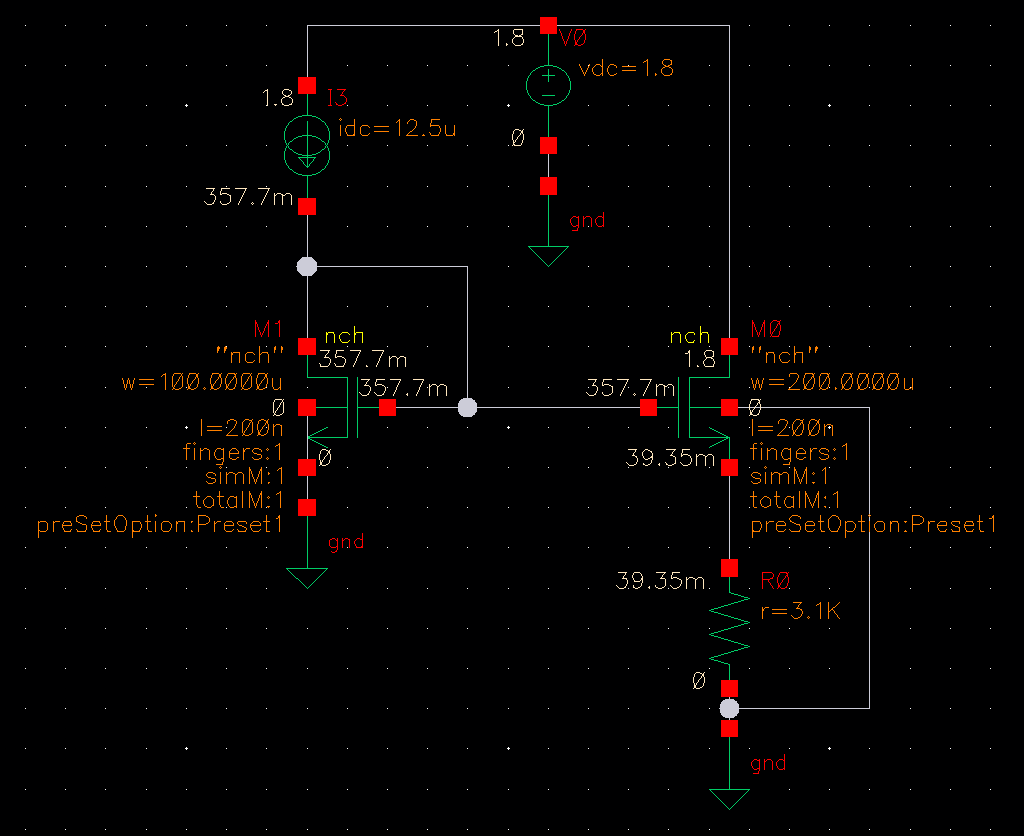
6/2/2023 – You want your reference circuits to take up very little power, so I’m thinking 10-20uA total current consumption. Looking through parameter sweeps, 12.5uA reference current seems like a good point, with 20/0.2 as a W/L ratio for M2. With a gm/Id of 25.8, gm should be 323uS, which means a resistor of 3.1k.
This means the source node of M2 will be 3.1k * 12.5uA = 39mV above ground. After some experimentation and simulation, I’ve found that it’s better to just make the W/L really big, so even if the W/L of M2 is twice as big as the W/L of M1, the corner/process variations work out better if you make them 200um/200n vs 2um/2n.
I think of 200um as being huge on a 1sqmm die, but when split up into fingers and multipliers over a 200nm length, that’s on the order of square picometers, which is 1um x 1um. So I think we’re good there, it’s okay to take up a little bit more space while keeping power to microamps and keeping performance good.
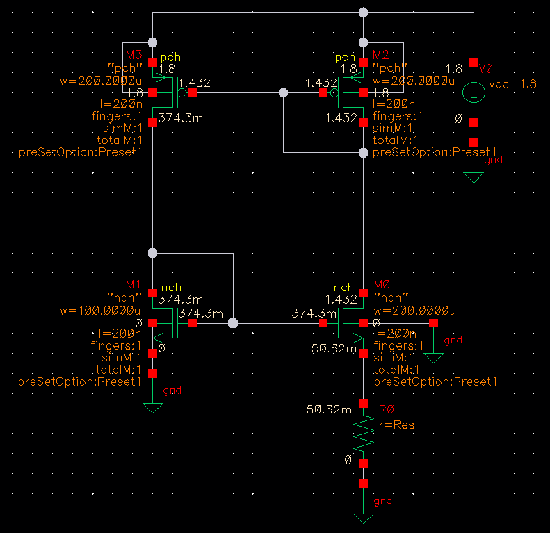
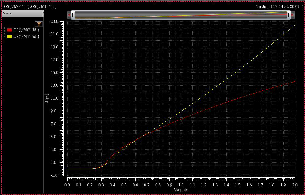
6/3/2023 – I run some PMOS sweeps and swap out the 12.5uA current source for a PMOS current mirror. Doing a sweep of the resistor, 4kOhms gets me closer than 3.1k.
This is a short-channel (submicron) technology process, so the sweep of supply voltage is *horrible*.
Next step is creating an error amplifier that can stabilize the reference. Baker recommends a gain of approximately 20-30dB. The PMOS transistors will be a load, but so will the startup circuit and anything connected to the BMR PMOS output voltage reference. I don’t know yet how many transistors it will be, but the Cgs (which will dominate the output load capacitance) of these transistors are on the order of 80fF or so. Therefore if I design for a load capacitance of 1pF I should be more than good, and I may even relax it down to 600fF. Pray I do not alter it any further.
My first step was using an ideal VCVS. Something was not lining up and no matter what I did , I could not get the error amplifier to complete the loop right and not get nonsensical values. But then I remembered that the whole point of doing this is to keep the drain voltages equal to each other to get around channel-length modulation effects. One way to do this is a cascode. While one of the benefits of a cascode is that it increases output impedance of an amplifier stage, the other is that it “protects” the transistor below it from drain voltage variation.
I added a cascode transistor to each branch, and it’s not great but it did instantly make it quite a bit better. I couldn’t figure out how to bias it though so I put a VCVS in to control the gate of *that* cascode, to create an ideal matched current source. I’m getting much better results, but I’m hoping this isn’t a stray “bad simulation”. Time to make the diff amp I intended and use it for this.
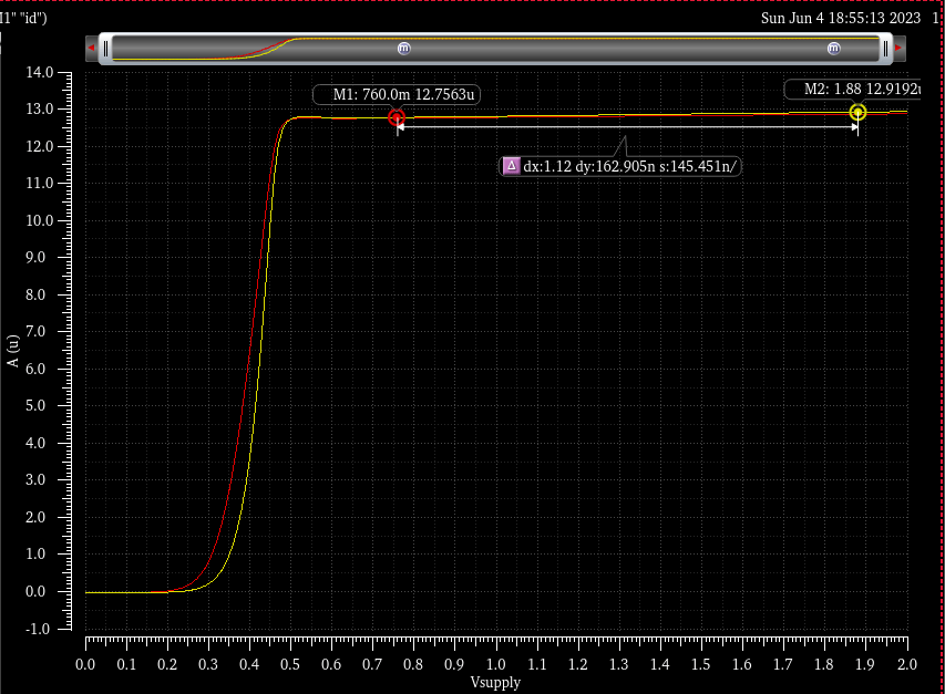
It is then in this moment…that I slap my forehead. I am such an idiot and I realized what I was doing wrong. The error amp works on the NMOS cascode and not the PMOS load because…my inputs were reversed. Once I made that simple swap, I got a *stellar* result. I’ve always said that my absolute favorite thing about engineering is when the theory lines up with experimental results. Look at this work of beauty, 0.62% variation around 1.8V, about 70nA/V.
6/4/2023 – When the amplifier has a gain of 10, the results aren’t as good, but Baker recommends taking the current mirror and making them both diode-connected. Trying this, I actually get significantly worse results, even with a gain of 100. So for this PDK I’m going back to the regular current mirror. I put together the differential amplifier, and characterize it just for posterity. It’s got a DC gain of 35dB and phase margin of just under 90 degrees — as is expected with a one-pole system with a couple non-dominant poles. The transition frequency is 100MHz, corner frequency of 1.8MHz or so. I would prefer a higher transition frequency, but it’s really entirely dominated by the output load. If I reduce the load capacitance to 100fF, we get 20dB gain at 100MHz, which means that we have a PSRR of 20dB at 100MHz. This may mean that every section of the circuit will need its own reference. But then the phase shift in noise between them will ripple throughout. I’ll have to look into that more later.
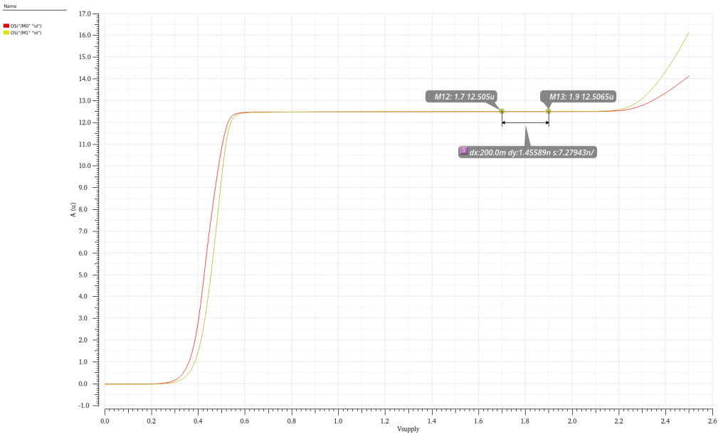
I add in the startup circuit, and we’re done! I think! Here’s the circuit:

And here’s the output current of each branch. That’s 7nA/V and just over 0.01% variation around 1.8V. I’m looking at 1.7V to 1.9V since that’s a 5% variation for a LDO/power supply. What’s interesting to note is the curve up there at the end. That’s actually from the startup circuit, and a W/L of 10/40 pushes that curve further up vs a W/L of 20/10 which makes the curve closer down to 1.2V which is well under our range.
For one final test I’m doing a step response on the supply voltage, so stepping from 0V to 2V on startup. I have to say, surprisingly, this is actually where I ended up learning the most. I’ve always wondered how they chose bypass capacitor values or really how they figured out any app notes and PCB level circuits for a certain IC.
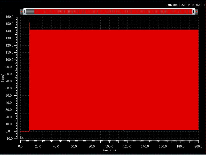
The first transient simulation was bad, and I tried changing the parameters and tuning it over and over but every simulation took minutes. If a transient simulation of a non-switching circuit takes minutes, ya done fucked up son.

The output transient graph was a bunch of spikes up and down every other nanosecond like this
Complete nonsense. I then remember that the amplifier was meant to work with a 1pF load, which it does not have. So I add 10nF caps to each output, VbiasN and VbiasP, and this is the resulting graph. It took roughly 5 seconds to simulate, which is how you know it’s okay.

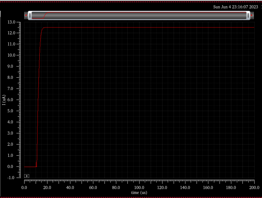
What I found to be the best combo is putting a high frequency RC filter on the VDD supply to begin with, which gives me an *excellent* step response and startup, 5 microseconds and it’s pretty much instantly stable, I love it. This is a straight up perfect step response.
This took 3 days, 2 of which were spent partying and at a Zed’s Dead show, but I’m super happy with this. It *only* took 3 days, which is a great time if you’ve read my other posts on this page. I really hope this helps me make more circuits, I’ll turn it into a hierarchical block to use elsewhere.
