To get myself back in the groove of analog design, I’m hitting the basics. The idea is to try out different topologies and play around with them and see the advantages/disadvantages of each with my own eyes, which will also help give me an arsenal of starting points for future projects. I also want to learn how to properly set up testbenches in Cadence so I can quantitatively benchmark these against each other.
Unlike most of my blog posts, the point of these won’t be to teach anyone anything per se, but just to show my progress and maybe to inspire others to try the same or show a glimpse of what analog design looks like to someone who might be interested. Some of the things I do and say might be straight up wrong, so proceed with caution.
#1: Basic Two-Stage
NMOS OTA with PMOS CS output, and Miller compensation. First I set up the two stages uncompensated, then added Miller compensation (ngl this took me longer than I’m proud of), and then picked one thing to improve. In this case I tried to lower power consumption so I could sprinkle this op-amp around generously.
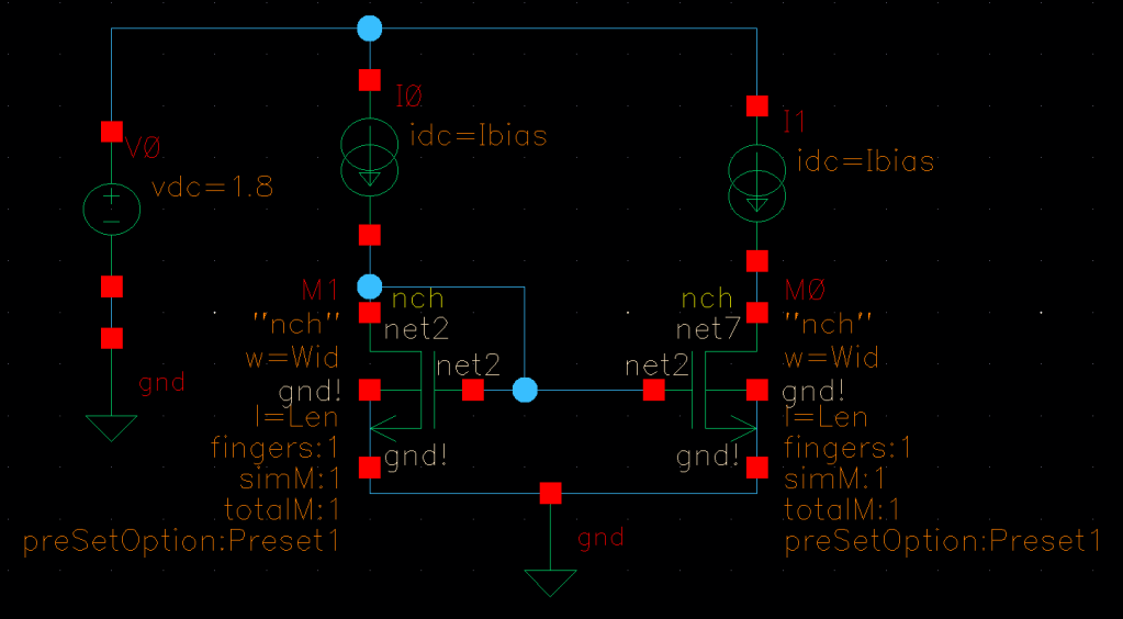
#2: High-Speed Telescopic Cascode
Next up is high bandwidth! I think what I’d like to do just before delving into ADC design is build an LDO, and for that I need an op-amp that has good CMRR and is very wideband so it can reject as much noise as possible. A lot about this project is learning how to properly bias and size transistors, so I’m not just learning this topology I’m learning more about analog design in general.

gm/Id for minimalists and idiots
I learned pretty quickly that the way I was doing sweeps was non-sensical and not very useful. I tried something akin to the gm/Id methodology for my telescopic cascode and it significantly reduced the amount of time it took to size transistors, I was hitting my targets on the first or second try within a few minutes. I tried taking it all the way and writing scripts to run through thousands of variations, but I found this to be waayyy overkill for my simple old tech node. So I found out a nice little medium point that I think will be useful for analog students designing with something like gpdk45 or gpdk180.
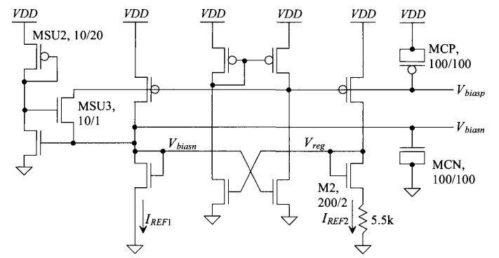
Beta Multiplier Reference & Biasing
As we discovered in my horrendous attempt at designing a telescopic cascode op-amp, issues in biasing can lead you to chase your tail for days and waste precious time that could go towards actually designing the core part of the circuit. Baker’s CMOS book strongly suggests numerous times throughout to create a “beta multiplier reference” (BMR) which then biases various other transistors or current sources. So that’s what I’m going to try here.
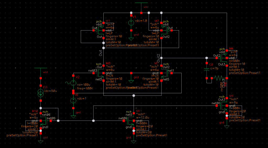
#3: Differential OTA with Common-Mode Feedback
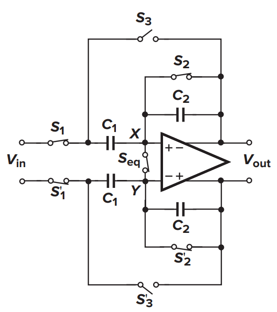
I want to use the BMR from the last post to properly bias a differential circuit, which is super important for any filter or switched-capacitor circuit. That means dealing with CMFB, my worst enemy (so far).