Printed Circuit Boards (PCBs) are the backbone of electronics, the land we build on. To the average person, when you’re thinking of circuits, you’re thinking of PCBs.
There’s a lot to say about circuit design, layout, signal integrity, safety, manufacturability etc. but I wanna get even more basic than that and describe what a PCB is made of. What the hell are we even talking about here?
Even though the vast majority of circuit design is done on PCBs, a standard university program will teach you nothing about them. So okay say you get a job and you know circuit theory and maybe you’ve even read a little bit of Art of Electronics, but you’re being asked to design a PCB and are totally lost. You look up tutorials on designing PCBs or how to use the EDA software, they’ll show you how to use the software, they’ll show you good layout practices, but it will feel like you missed a lecture at some point somewhere. What the hell is a solder mask!??
This is exactly how I felt when I first started out. It’s important to get an understanding of what they PCBs are and how they’re made if you’re ever going to put circuits on them. This is going to be a very simplified overview but hopefully by the end you’ll know enough to work your way through using CAD to actually make something you can hold in your hand.
Why PCBs?
PCBs are a tidy and streamlined way to implement a circuit at low cost. Like think about the difference between a clay pottery bowl you make by hand and paint, vs. a ceramic bowl you can buy at the store. One has more character and makes for a better gift, the other can be made quickly and cheap and is exactly the same every time. Shit, I just remembered I still haven’t done my Christmas shopping.
You can always grab a battery and wires and resistors and just solder them up in free space, not secured to anything. There’s a popular method of building circuits at home called “deadbugging” (named because the ICs look like dead bugs) where you just glue components upside-down to a piece of wood and solder them up, or cut up copper cladding and solder to that. Below is a circuit I quickly made on copper cladding to flash some LEDs for a trade show demo. It’s a completely valid way of putting together a circuit, I mean who cares as long as components are connected together right?
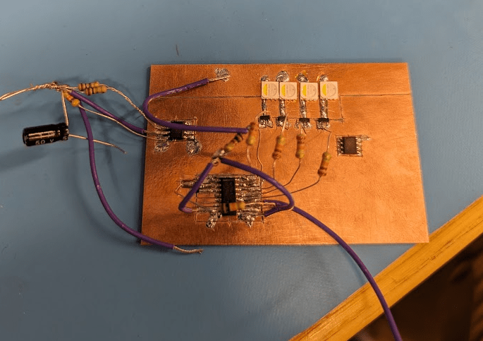
This works better than you’d expect and is a fast way to prototype concepts, but obviously not a great way to get reliable circuits you can quickly put together in volume. This was fast in the sense that I went from concept to demo in a couple hours, but it was one (1) unit and I burnt my fingers a couple times. You can only burn so many fingers before you give up your childhood dreams of mass manufacturing cost-efficient embedded systems and look to alternative avenues.
PCBs allow you to create clean, compact, reproducible circuits that are easy to assemble.
The data is digital (Gerber or ODB++ file formats), and they’re produced in large volumes within very tight tolerances by an assembly line. It’s so sturdy. The drawback is that they are permanent, etched in metal, meaning you can’t rework or re-use or recycle for other purposes. This leads to the very serious and sad problem of e-waste.
Ogres are like PCBs; they have layers
PCBs are made up of different layers of material which are individually fabricated and then pressed together.

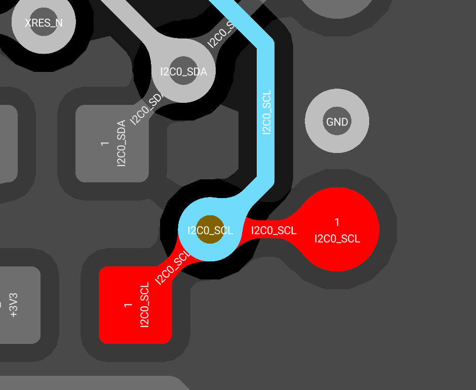
Even though our circuit board is flat and thin, like a 2D plane with some components on top and bottom, it’s actually a very complex 3D structure. The copper layers are for electric signals to travel through, while the dielectric layers keep the different copper layers separate from each other (NB: the EM waves travel in the dielectric between the copper, the copper is a waveguide, but that’s not important right now). Below is a single highlighted trace that connects two components together.
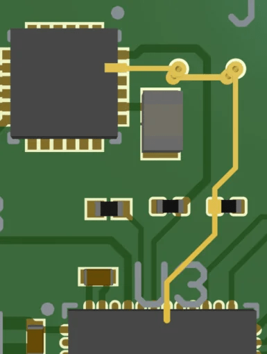
You can see how it goes from one chip and then down a via then over then up another via then hits a resistor before connecting to another chip. Interwoven between other copper traces and planes, while the dielectric layers give it structure and space. “Traces” are the equivalent of wires in a PCB, copper lines etched onto the fibber-glass layers. You can spend a lot of time carefully drawing these.
Different copper layers are usually for different purposes. Some layers are one continuous plane of copper, used as the ground plane or to distribute power. This is both to provide a clean, low-impedance connection for all your components, but also for simplicity and ease of design. 4-layer boards are so cheap that the time spent manually drawing out ground and power connections between all your components in a 2-layer board is rarely if ever worth it. Just throw in a ground and power plane
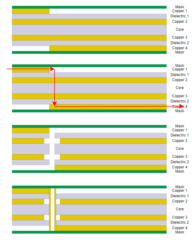
The order and thickness of those layers is called a stackup. This is what a 4-layer stackup looks like, a cross-section of a PCB.
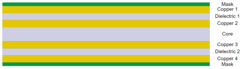
Looks kinda tasty doesn’t it? Metallic sandwich! Keep in mind that this is actually only 1 or 2mm thick. Like about the thickness of a stroopwafel.

There’s a few layers of conductive material, which we can etch and shape into traces to connect components to each other. There’s layers of dielectric to keep them safe and separate and cozy. Usually some type of fiberglass, FR-4 is the most common. There’s solder mask and paste layers.
Engineers design the board as a whole, but the information is sent over layer by layer because they’re manufactured layer by layer. The layers are then pressed together and laminated, and holes are drilled and filled with copper to connect layers between each other. The number of layers and the way these layers need to be connected may require multiple iterations of pressing and lamination, which can lead to the fiberglass getting crushed and causing defects. You’re usually limited to 4 press-lamination cycles at most.
Knights of the Round Copper Pad
Copper has one big huge giant shitty issue: it oxidizes. It happens pretty much immediately, and it degrades the copper and makes it more difficult to attach components to it. A PCB is worthless if you can’t use it to hook up components somehow.
We have one final step before we have a finished PCB, and that is plating or surface finishing. Plating is a simple idea but not necessarily easy to execute and it becomes a web of silliness.
Copper oxidizes when exposed to, hey wow, oxygen. Not great considering oxygen is everywhere. What we can do is immediately cover the copper with some other material. The two primary ways are “hot air solder layering” (HASL) and “electroless nickel gold” (ENIG) plating. By applying one of these, the copper is protected from oxygen while components can still be soldered on comfortably and reliably and conduct current.
HASL is where the PCB is straight up dipped into a pool of molten solder. Quick, dirty, cheap, and since it’s solder it’s naturally easy to solder components to. ENIG is a bit more complicated and thus more expensive, but you can get a suuuuper flat finish which is perfect for attaching chips with dense pin arrays. Gold is conductive and easy to bond to and completely resistant to oxidation, but it doesn’t really stick to copper so well. Nickel is conductive and sticks to things well, but its not great for bonding and is also prone to oxidation. The compromise is plating the nickel over the copper, and then plating gold over the nickel, to get the best of both. There’s multiple other options and variations but these are the two main ones you’ll encounter.
Vias
Okay so at this point we have all of our layers. We have the layer stackup which defines dielectric and copper layers where the signals and power go. We’ve got plating to protect the surface copper. These layers are not particularly useful in isolation, so to make them work together as one cohesive 3D structure we connect them with drilled conductive holes called vias.
Vias are just pathways to connect the different copper layers, a simple concept, but by far the worst part. PCB via size and spacing is often the singular bottleneck in electronics packaging. It’s a common technique to use FPGAs as nothing more than interconnects rerouting dense digital signals because vias can’t be made dense enough.
Let’s say you have a component on one side of the board, and you need to connect it a component on the other side. You also need to connect these components to power and ground, which may have their own layers. If you have multiple ground layers, those ground layers all need to be stitched together at as many points as possible to get a nice even reference voltage. A typical board has hundreds if not thousands of vias. They have resistance and inductance and require careful attention, do not treat them lightly.
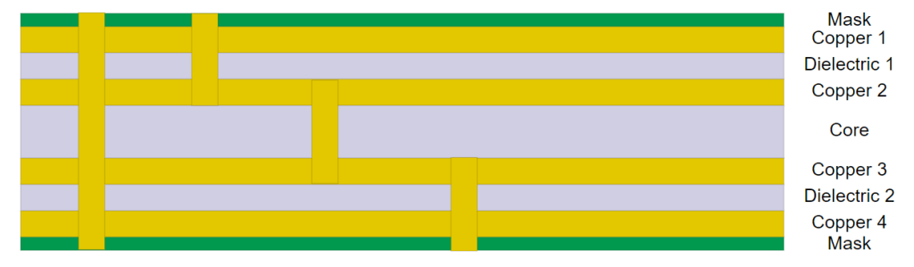
Let’s take an example of needing to connect an ADC on one side to a microcontroller on the other side. The board would have to be flattened and drilled and connected like so.
Look through those steps again. Think about what they mean, what’s involved, where it can go wrong and where we can set it up for success. Each layer is designed with a plan for where a hole will be drilled on that layer. Each layer is individually fabricated, and etched. They’re drilled, either mechanically or with lasers. Groups of layers with their vias connected are pressed together, and those vias are often filled with conductive material like copper or silver epoxy to wire them up.
There’s some interesting things to note here. These vias are mechanically drilled. That means that your via sizes need to match the drill bits available by the fab house. That also means that the more sizes you use, the higher your tooling costs. If you just make all your vias the same size, say 0.2mm or something, you reduce your tooling cost and also make the design simpler.
We don’t make the hole and then put copper around it. The way it looks in this screenshot makes it seem like we make the hole and then put copper around it. That’s how we think about it when designing, but that’s not what happens in manufacturing. In reality you’re making copper pads (or empty voids) that all line up on different layers and then drilling somewhere in the middle of that. On the layers where the via is connected to copper, it needs some extra copper around it since the drill won’t have 100% accuracy and might be off-center; this is called an annular ring. On layers where the via is not connected, there should be a certain clearance from any copper.
Here’s another puzzler. In the diagram above we drilled from layer 1 to 4. What if we want layer 2 to 3? Or 1 to 3? Or what about a signal that goes 1 to 2, travels for a bit, then goes 2 to 3? Is this even possible?
Well this depends on how we set up our via pairs. Via pairs are the layer combinations that are being drilled. We can set up our via pairs in such a way as to reduce cost and be smart about it.
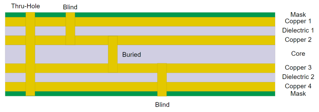
Let’s take the most extreme example, where we want vias between every single pair of layers. So that’s a via from 1:2, 2:3, and 3:4. How would this realistically get manufactured? Well, layers 2 and 3 would first be pressed together and laminated and drilled 2:3, then layers 1 and 4 would be pressed and laminated onto that and drilled 1:2 and 3:4. This is 2 lamination cycles and 3 drill cycles. These are also what are known as blind and buried vias. Blind vias start from the surface and are “blindly” drilled in, buried start and end somewhere in the middle.
While this is possible or even mandatory in certain situations, it can be outrageously expensive. On top of the fact that it’s extra processing steps which can also increase the failure rate, when you drill between layers that are directly adjacent (like 1:2) you may need to use laser drills so you don’t accidentally drill down to layer 3 and cause a short. Laser drills only come in one size and adds tooling expense.
If possible, it’s best to just use the 1:4 layer pair (a thru-hole via) for all layer changes. If you want to go from 2:3, you do one 1:4 thru-hole, and leave the via disconnected on layer 1 amd 4. The upside is that this is cheaper and less prone to failure. The downside is that any signals on layer 1 and 4 have to go around this via, which can make routing difficult if it’s dense with traces and vias.
Stencils! Solder! aSsembly!
The board is complete, we have a Printed Circuit Board. But the story isn’t over.
The whole point of a PCB is to provide easy convenient connections between components in a way that keeps them all glued together. The PCB provides (a) a rigid mechanical surface for components to sit on and (b) a pathway to connect them. That’s our goal, and everything about PCB design is purely about facilitating those two things. We now need to turn a PCB into a PCBA (printed circuit board assembly).
Components are attached to the board with solder. Solder is a conductive alloy that can be melted to create a permanent joint between components and the board. There’s a dozen different types, various alloys that come in different forms like wire spools or paste, and typically categorized as with or without lead. If you’ve ever seen “RoHS”, that means the solder is lead-free, which maybe makes it safe to eat but I haven’t tried. You put the component down on the copper traces where you want to attach it, matching the component’s pins to the PCB pads, hold some solder to it, and then apply some heat (more on that later). You can do it yourself with a hot iron tip or hot air gun, but industrially these are placed in an oven or other contraption. The solder also needs some flux to clean the surface and help the solder flow nicely.
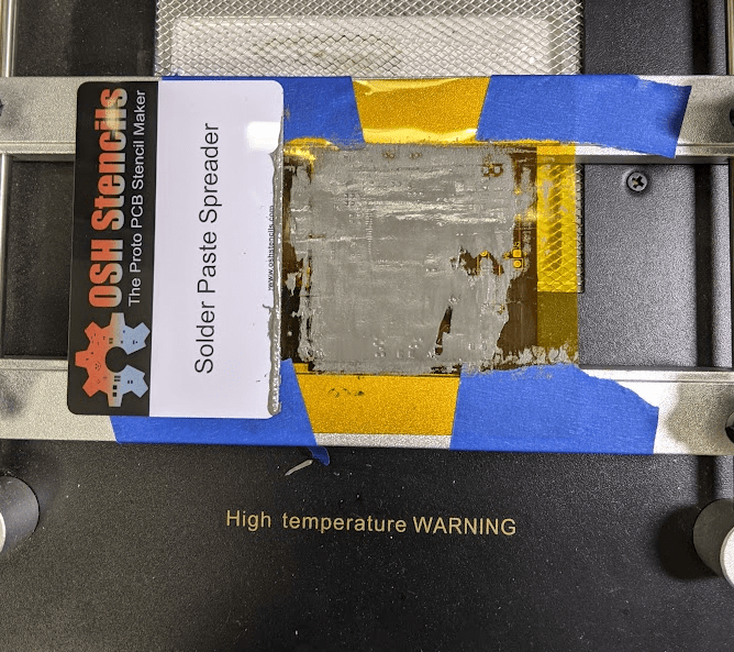
For surface mount components, they solder paste where the metal is like these teeny tiny pellets suspended in the glue. In your PCB design software, you designate a paste layer which is used to create a stencil. This stencil only needs to be made once, and the fab house holds onto it for future runs. After the PCB is manufactured, the stencil is held onto the PCB, and paste is squeezed onto it and scraped off. You can even do it yourself, like I did as shown below.
There’s an issue here though. If you were to etch copper onto FR-4, squeeze out little dots of solder paste exactly where you want the components to go through a stencil, place components, and apply heat, you’d get an absolute mess. I mean, look at that microcontroller with like 100 pins all bunched up next to each other. How does the paste not all become one pool once melted?
See, liquid solder has surface tension like water. It’s going to go where it wants to go. We have to guide it by adding a blocking layer, a dam. By blocking off everything but the pads, when the solder paste melts, it stays on each pad exactly within that pad. The drawing layer designating where this blocking material should and shouldn’t go is called the solder mask layer.
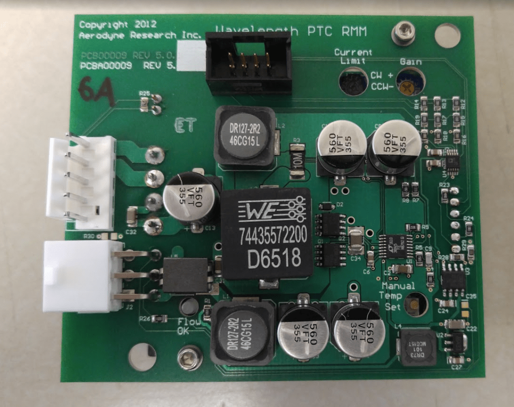
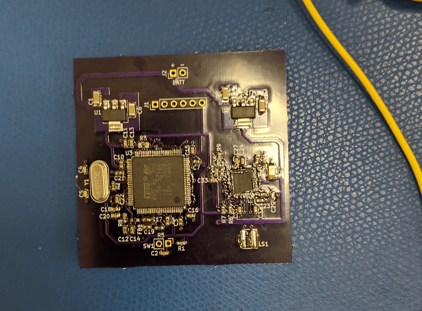
The solder mask is what gives PCBs their signature green color. The picture above is a prototype board I got from OSH Park, who uses a purple solder mask. Green is the cheapest though so it’s what most of them are.

After paste is applied, components can finally be placed. For prototype boards, you can place them by hand with tweezers, but in volume production it’s done with a Pick And Place machine. Took them 3 years of market research to come up with that name. The assembly house receives a Bill of Materials (BOM), and pick-and-place file which has x-y coordinates and orientation of placement for each part, they buy the components and feed the reels into the Pick and Place machines. The advancement of Pick and Place machines has been the key to reducing board sizes and increasing density. They can place components that are 0.1mm on each side to high accuracy, components so small that they may need glue applied to them just so they don’t fly off when soldered, at a speed of 10s of thousands of components per hour.

Once components are placed, they’re set to go in the oven, time to do some baking 🙂 They go into a special oven called a reflow oven, which is meant to heat up all the solder paste evenly to a nice crispy 200-250C so it all melts at the same time. When the solder paste melts, it creates surface tension which pulls the components down. If you have a hot air gun and do it yourself you can see it happen as well, it’s a very satisfying thing to see. If all goes well, we’re done! We have a fabricated board assembled with components on it. The assembly house performance inspection and carries out quick electrical testing and ships it to you all packaged up.
The whole shebang
We’ve covered a lot of ground, it’s worth reviewing the major steps:
- Engineers send the design files for the various layers (copper, paste, solder mask, drill drawing etc.) to the fab house in either the Gerber or ODB++ file format
- The fab house checks these files, and converts them to the formats their machines need
- Copper is etched onto dielectric sheets
- These layers are pressed together and laminated
- Holes are drilled and filled to create vias between layers where traces, planes, or components need to connect to each other, and shapes/slots/grooves are cut out of the board as needed
- Steps 3-5 are repeated until the full layer stack is complete
- The surface is finished with HASL, ENIG, or some other plating
- Boards and components are shipped to an assembly house
- Solder paste is squeezed onto pads through stencils
- Components are placed by a precise Pick and Place machine
- The boards are baked in a reflow oven, like cookies 🙂
- Pop some champagne for a job well done, plug in the board, and promptly get flung backwards by an explosion due to a minor oversight
It really is that simple!
Final Remarks

PCBs are highly complex and a lot more involved than you’d expect. The people designing them and the people making them are worlds apart, to the point that as far as I know, no company fabricates its own PCBs in volume, whether it’s a small shop of 10 people or a megacorp like Apple. Seriously, think about that. Companies like Samsung manufacture their own chips, a process that costs billions of dollars. And yet Apple, which owns as much of its manufacturing as possible and now even designs its own chips, outsources its PCB manufacturing.
There’s so many more details and features to cover, things like advanced assembly such as wire bonding and flip-chip, paneling and a variety of mass production tricks, impedance control, high-frequency substrates like ceramic, electro-optic co-packaging, flexible circuits, creepage for high-voltages, and others.
Hopefully this article, which I think may be my longest yet, gives you a rundown of the basic terminology and concepts enough so that when you approach a design, whether its to understand something someone else made or to make your own for the first time, you’re not overwhelmed. It’s just layers, dude 🙂
