Transimpedance amplifiers (TIAs) find wide use in electronics and systems, from things like optical communication transceivers in WiFi routers, to electron multipliers in mass spectrometers. They’re one of my favorite basic subcircuits to design. They’re often used in situations where you’re trying to squeeze water out of a rock (our TIA at Bruker for mass spec was measuring just a few individual electrons worth of current), so you have to really know and love op-amps up close, non-idealities and everything,
Analyzing a TIA’s bandwidth is an exercise that may introduce some less experienced readers to new concepts or perspectives needed for analog design.
Let’s start with the basics. A transimpedance amplifier takes a current input and converts it to a voltage. The simplest TIA is in fact just a resistor. If you take a resistor and put a current through it, you get a voltage. A lot of high tech optical comms TIAs are just a resistor and transistor, nothing else. Simple, fast, and usually unconditionally stable.

In communication schemes, the optical signal is digital (light is on or off), but in many applications especially at the PCB level the signal is analog. In those situations, it’s important to keep the photodiode biased at a steady known DC voltage. This is because the DC voltage bias affects the sensor’s depletion region, which directly affects many of its qualities. That leads us to the popular op-amp-based shunt-feedback transimpedance amplifier.

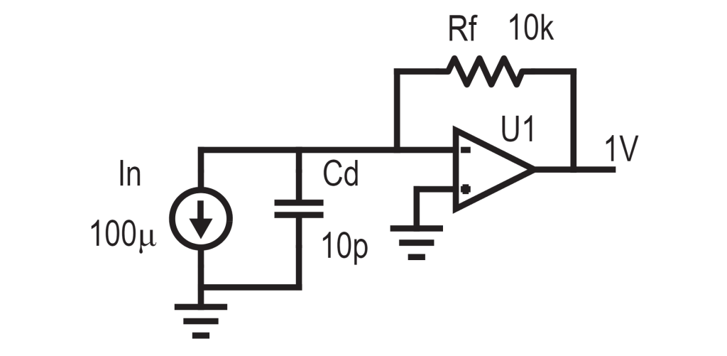
For those of you who have heard of TIAs, this is probably the form you’re used to. We have a photodiode, with one end tied to -3V. What’s the voltage at the other end? Well that’s set by the op-amp. The op-amp’s positive terminal is ground, and because it has valid feedback, it’s negative terminal is also going to be held at ground. Therefore the photodiode is reverse biased with 3V across it. A regular diode is a passive device that conducts current only when forward biased, but a photodiode produces current when reverse biased. Neat-o. This configuration also provides considerable benefits to the bandwidth, which we’ll get to later.
Little to no current goes into the input of the Op-Amp, so according to Kirchhoff’s Current Law (aka conservation of matter) all the current must go up through the feedback resistor. Per Ohm’s law, the output voltage is simply the photodiode current times the resistor.
Feedback and Gain
A typical amplifier has a gain with units of V/V (yes seriously, volts per volt), otherwise written in dB. A transimpedance amplifier however is V/A, which happens to be the definition of Ohms. Impedance is in the very name so it makes sense.
In the TIA below, the feedback resistor is 10kOhm so the gain is simply 10kOhm. A 100uA input current would get amplified to a 1V signal.

We’ve previously discussed feedback factor and how it relates to bandwidth, but that was for a regular voltage amplifier. What’s the feedback factor here and how does it affect the bandwidth?
You would think that if the gain is 10k, the feedback factor is 1/10k. If that were the case, the bandwidth would be divided by 10k. A 1GHz Op-Amp (which is super duper fast) would end up being only 100kHz, which is hilariously slow.
Unlike gain which can have units of V/A or A/V, feedback factor is unitless. In this case, our input signal is current, so we actually want to just analyze it from a current perspective. When you look at it that way, it becomes obvious that the feedback factor is just…1. Any input current is being fedback in exactly the same quantity by the Op-Amp, which means that a TIA is just a current-mode unity gain amplifier. That’s one of the nice things about TIAs, they can have very high transimpedance gain without taking a hit to bandwidth.
Push it to the limit. The limiiiit!
Unfortunately the first pass is just that, a first pass. There’s some realities we need to deal with. TIAs are more often than not used at very high speeds. I’m talking anywhere from hundreds of MHz to tens of GHz, it can get messy. We need to know the realities so we can bend our circuit around them and push it to the limit.
There’s the input bias current, there’s the input offset voltage, there’s the finite gain of the op-amp, there’s its limited bandwidth, noise, temperature drift, and all its parasitics.
The non-ideality that matters the most and will be our focus of analysis here is the parasitic capacitance of the photodiode. It’s important to understand that this capacitance is built into the photodiode, all p-n junctions in fact.
How does this change our analysis? Let’s go back to the initial perspective, current. The capacitor and feedback resistor appear as a current divider. As we go up in frequency, the capacitor becomes a smaller and smaller impedance, so more of the input current goes through it and not the feedback resistor, effectively lowering the gain of the amplifier. In other words, the photodiode’s parasitic capacitance limits the bandwidth of the amplifier.
Now there’s another very important and interesting perspective we need to view the circuit from. We only looked at what happens from the inverting terminal, but how about the non-inverting terminal? That seems silly, the non-inverting terminal is at ground, there’s nothing there.
But that’s actually not true. There’s NOISE at that terminal, and that noise gets amplified. We must analyze this voltage source at the non-inverting terminal differently than we analyzed the current source at the inverting terminal.
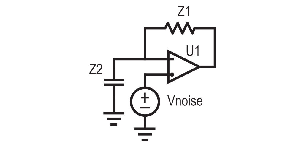
The gain of a non-inverting op-amp is 1+Z1/Z2. In this case, Z2 as a capacitor becomes smaller as frequency goes up, leading to increased gain. So as frequency goes up, the noise gets greater and greater, eventually drowning out the signal and rendering the amplifier useless.
The zero can also cause stability issues, as the phase margin is completely destroyed, or the gain never goes below 0dB so there’s always potential for oscillation at some frequency. To alleviate this, we will often add a capacitor in parallel with the feedback resistor to introduce a pole near the zero and manage the frequency response, keeping it stable.
So what’s going on here? We have two separate transfer functions? Yup! The input current signal is amplified by the signal transfer function (STF), while the noise is amplified by the noise transfer function (NTF). This is particularly an important topic in noise-shaping ADCs (such as a Delta-Sigma ADC), which are very cleverly designed to attenuate noise while amplifying signal, thus increasing the signal-to-noise ratio (SNR) as opposed to most amplifiers which provide gain to signal and noise equally.
The Inverting Op-Amp – A TIA in a Wig
Something you may notice about our analysis of noise transfer function vs signal transfer function is that they sort of resemble the inverting op-amp vs non-inverting op-amp.
And that’s because, as a matter of fact, the inverting op-amp is actually a crappy TIA. A non-inverting op-amp feeds the output back to one terminal through a voltage divider, which it compares to the input voltage on the other terminal. In my previous post on feedback factor, I remarked how the gain formula for an inverting op-amp is different because the input signal has a “feedforward” divider, and that has to compensated for. But another “truer” way to look at it is that the inverting op-amp is really feeding back current. Now what about the frequency response? Our original TIA had a feedback factor of 1 and therefore the bandwidth was pretty wide. We know for a fact that the inverting op-amp’s frequency response changes with gain, so clearly it doesn’t have a feedback factor of 1. A way to look at it is that the voltage source and R1 are a Thevenin source, which we can transform to a Norton source. Now you can clearly see that the current is actually being divided, and the feedback factor is no longer 1, and therefore the bandwidth is affected. Pretty neat huh?

Once you do that transformation, you can apply the same logic from the TIA and see that the inverting amplifier and non-inverting look exactly the same from a noise perspective. The inverting and non-inverting amplifier have the same noise transfer function, but different signal transfer functions. But the inverting amplifier requires a smaller feedback factor for the same gain as the non-inverting, which means more noise. You can readily see that if you were to make an inverting amplifier with a gain of -2 and a non-inverting amplifier with a gain of 2, the inverting amplifier is fundamentally noisier, because from a NOISE perspective it looks like a non-inverting amplifier with a gain of 3, so noise is amplified by 3 while signal is only amplified by 2.
Conclusion
TIAs are so compact and simple, and yet reveal so much about circuits and design, both in theory and in practice. They teach us about signal and noise transfer functions, about stability, feedback factor, bandwidth, the different types of feedback, and how seemingly trivial non-idealities can cause massive headaches. But if you can get it right you can make those things *sing*, it’s a very rewarding feeling.
Speaking of compact and simple: