Today, we’re going to build a single transistor amplifier, just to show you that the theoretical numbers and models you use in class do in fact serve a purpose.
Okay so let’s start with the premise. We want to create a single transistor amplifier that has a gain of 10, and works off a 9V battery. 9V batteries don’t have a long life-span, so we’ll keep the quiescent current — the current drawn even when there’s no signal — in the 100uA range or so.
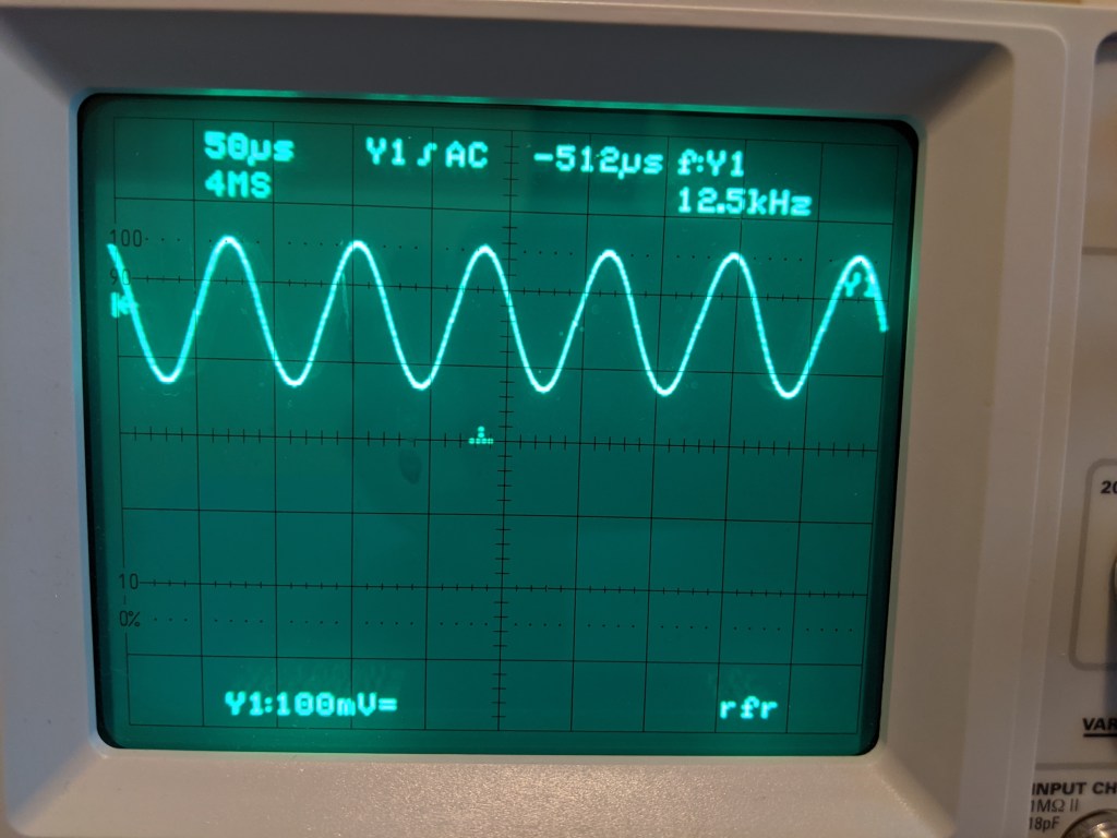
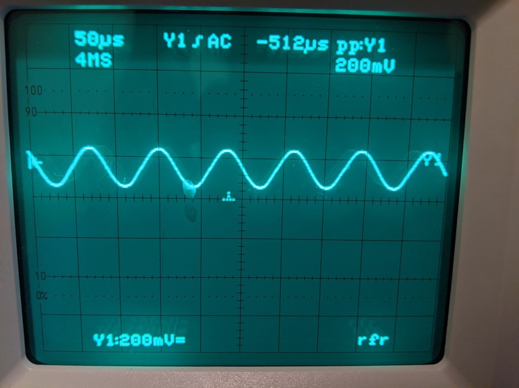
The input test signal is coming off my microcontroller, an STM32F407. I’m using its DAC to output a sine wave with an amplitude of 100mV @ 12.5kHz, or 12Vpp. The whole wave has to be positive, so I offset it by +100mV. Aaaand…
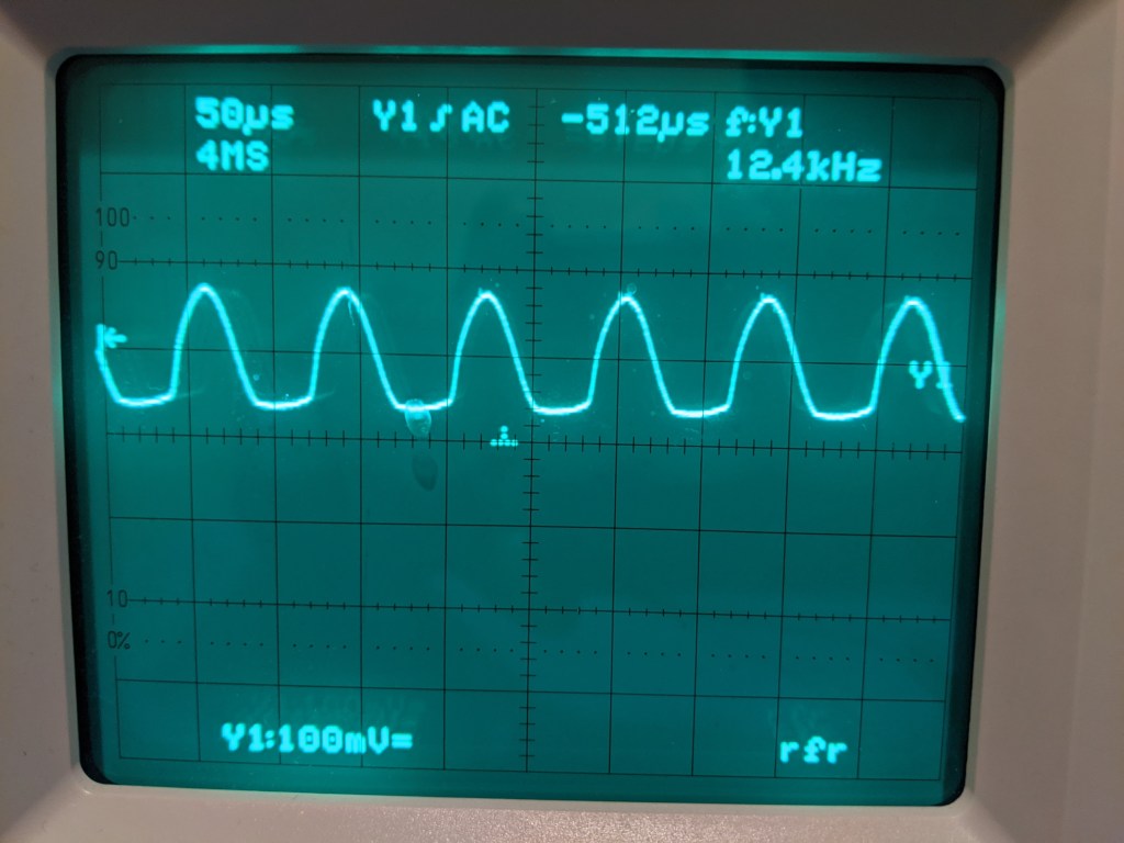
Wait a minute what the hell? I double check my data, I check my code, make sure it’s all operating as expected, then try a different scope channel, check with the multimeter and yup it really is refusing to go below 20mV. Hmm, maybe there’s something in the datasheet?
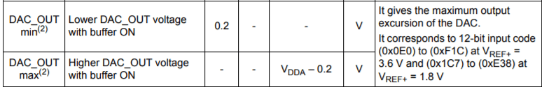
Of course there is! Look at that. Minimum spec is 200mV, so we’re doing great! But that’s not good enough. Now, I could turn the buffer OFF, which gives me a minimum output spec of 0.5mV, but then I gotta deal with different impedances, and you know, I just do not care to do that right now. I don’t have a function generator in my apartment, sue me, so I’ll just increase the DC offset and be done with it. We’re gonna use a capacitor to take care of that DC offset anyway a.k.a. “We’ll fix it in post.”
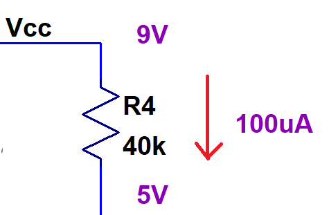
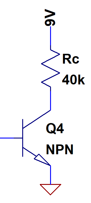
Alright, now that we have our dummy input signal taken care of, let’s turn this into an arbitrarily useful output! In general, you want to center the output right around half of Vcc, but shifted up a little. The reason is that the BJT’s collector voltage needs to remain a little above GND so the BJT can remain in the forward-active region, so your output swing can’t go all the way down to 0V. That restriction doesn’t exist for the upper rail, it can go all the way up to 9V no problem. So let’s center the output around 5V. 9V-5V=4V, which with a 100uA quiescent current means a 40kOhm resistor.
So far we haven’t touched the transistor at all. For a single transistor amplifier of this application, the Common Emitter is our go-to. We call it the Common Emitter because the Base is the input, the Collector is the output, and the Emitter is the Common reference between them.
If we leave the circuit as is (left), we run into an issue. The current coming down through Rc has an exponential relationship with the voltage at the base. So any issues that occur in biasing or noise or whatever get exponentially applied to the output. That spells trouble in the form of non-linearity. So what do we do? We can put in a resistor between the emitter and ground to act as a “shock absorber”. So even if the base voltage is subject to unwanted changes, the emitter is too, and the base-emitter voltage remains relatively stable. We call this amplifier a Common Emitter with Degeneration.
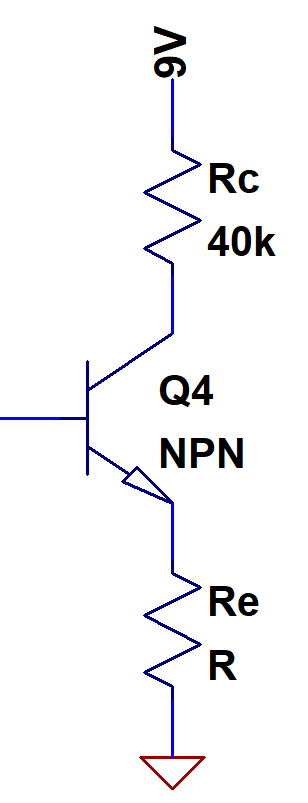
If we assume the transistor has a high current gain Beta, then *most* of the current going through Re is coming from Rc. What that means for us is that rather than directly controlling the collector current with the voltage at the base, we control with the voltage at the emitter, which is going to roughly be one diode drop from the base.
Speaking of base, we need to take care of biasing it. If we want there to be 5V at the output and 100uA going through the transistor, we’re going to need to have some fixed voltage at the base to keep that baby running. The simplest way to do this is with a voltage divider. Now, normally a voltage divider can’t be used to set a reference. The voltage divider equation is really a shortcut for a KCL equation where all the current going through one resistor can only go through another resistor. Once any of the current goes somewhere else, the KCL equation changes and your voltage divider no longer holds. In this situation, the current drawn by the base will remain relatively small. We’ll still account for it, but we can at least start by assuming the voltage divider formula.
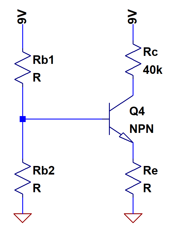

Now to input our signal. If we just connect the input directly to the base, that screws up pretty much everything we’ve been going for. The biasing divider won’t matter at all, and it’ll possibly even break our poor lil’ BJT. Plus the dummy input signal still has that pesky DC offset. We have an AC signal we want to pass through, but we have a DC offset we *don’t* want, while we also have a DC offset from Rb1 and Rb2 that we *do* want. How do we make this happen? A simple capacitor will do! After a short time (a really short time), the capacitor holds a DC voltage, kind of like a bouncer holding two drunken brawlers apart, and only lets their shouting AC signals through. We call this AC coupling. And with that, we have our completed topology.
But we don’t have a circuit. So far we’ve been talking in terms of concept and intuition. We need numbers, values to input. With that: let’s begin our calculations.
We’ve defined our desired gain, Av=10, our supply Vcc=9, and bias current Ic=100uA. The gain equation for a degenerated common emitter is Av=Rc/(1/gm + Re). We have Av, we have Rc. gm is the BJT’s small signal transconductance, kind of like the inverse of its resistance. As we’ll discover in another blog post, semiconductors are non-Ohmic, meaning they don’t have a normal resistance, instead we have gm, which is the collector current divided by a constant, known as the “thermal voltage” (roughly 26mV at room temperature). That gives us an Re of 3.74kOhms.
As we make these calculations, we’re going to make some assumptions that will simplify the process to get us close enough. Assumption #1: the current going into the BJT’s base is negligible, therefore the current coming out of the emitter is the same as the current going into the collector. If that’s the case, well then the voltage across Re is just the quiescent collector current multiplied by Re, giving us Ve=374mV.
Okay, this is where things get hairy. The BJT I have is the ever popular 2N3904, the golden retriever of transistors. It’s the one that comes with every kit, including the simple little SparkFun kit that I happen to have so let’s just go with it. There’s two main equations that come to mind with BJTs.

Ic, Ib, Vbe, and Vce are circuit parameters, and Vt is a constant. What we have left are Beta, Is, and Va. Va is the Early Voltage, a sort of parasitic resistance. When we operate the transistor as a switch, we assume a constant current through it, but the Early Voltage makes that current dependent on the Collector-Emitter voltage. A typical Early voltage is 100, so with 5V at the collector we’ll say it acts as a 1.05 multiplier. So then we have Beta (often shown in datasheets as hfe) and Is, the reverse saturation current.
Beta is generally given in the datasheet, because it’s easier to test for, but it’s not useful for designing an amplifier. A quote that really helped me “get” BJTs comes from the Art of Electronics by Horowitz & Hill: “A circuit that depends on a particular value for beta is a bad circuit.“
If we use the transistor as a switch, it gives us an okay idea of what current will be expected from the source. Beta is not a reliable value, and Ib is not something we can reliably control on the signal level, so it’s kind of useless for us at the time being.
That leads us to the second equation. The problem here is that Is is not given in the datasheet, and finding it is not a trivial task. Is is on the range of 1E-16 or 1E-14. Orders of magnitude. But at least this equation uses Vbe, which is something that we have greater control over, and when we solve for it, we’re using the logarithm of Is, so Vbe only changes by a couple dozen mV. The SPICE model for the 2N3904 tells us Is is 1E-14, but I’m not sure I trust that for real components. Assumption #2: Is = 1E-15. We solve for Vbe which gets us 615mV. If Vbe is 615mV, and Ve is 374mV, then Vb = Ve + Vbe = 989mV.
989mV is about 11% of 9V. That will be the ratio we want our bias network to have. We want to limit the current drawn by the bias resistors, so we arbitrarily set the upper resistor Rb1 to 100kOhm. We use the voltage divider formula and work it backwards to get Rb2 at roughly 12.35kOhm.
As I mentioned earlier, now is when we have to consider the fact that the biasing network isn’t really a regular voltage divider. Some of the current goes through the base of the BJT. Even if it’s a small amount, we will have to tweak our values. The current through the base, which then ends up going through Re, makes Re *appear* as a resistor equal to Beta times Re in parallel with Rb2. Beta isn’t a very reliable value. Here’s what the datasheet shows. Do you see what I mean?
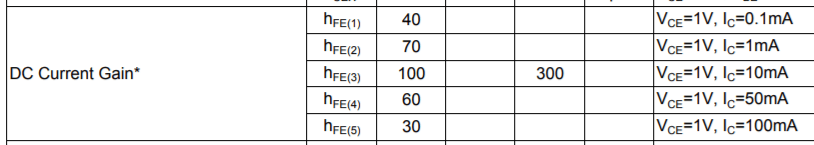
We get a really wide range of 100 to 300, but only if the bias current is 10mA. If the bias current goes up *or* down, the Beta drops, but we don’t really know to what. I defer to the SPICE model for a Beta value, which is 300. I don’t believe that to be a realistic value for our situation, I think it’ll be lower than that considering our bias current is 0.1mA. Assumption #3: Beta is 200. I work the parallel resistor formula backwards and find that Rb2 needs to be about 12.6kOhm when adjusted for the base current. With that, here it is, our circuit!
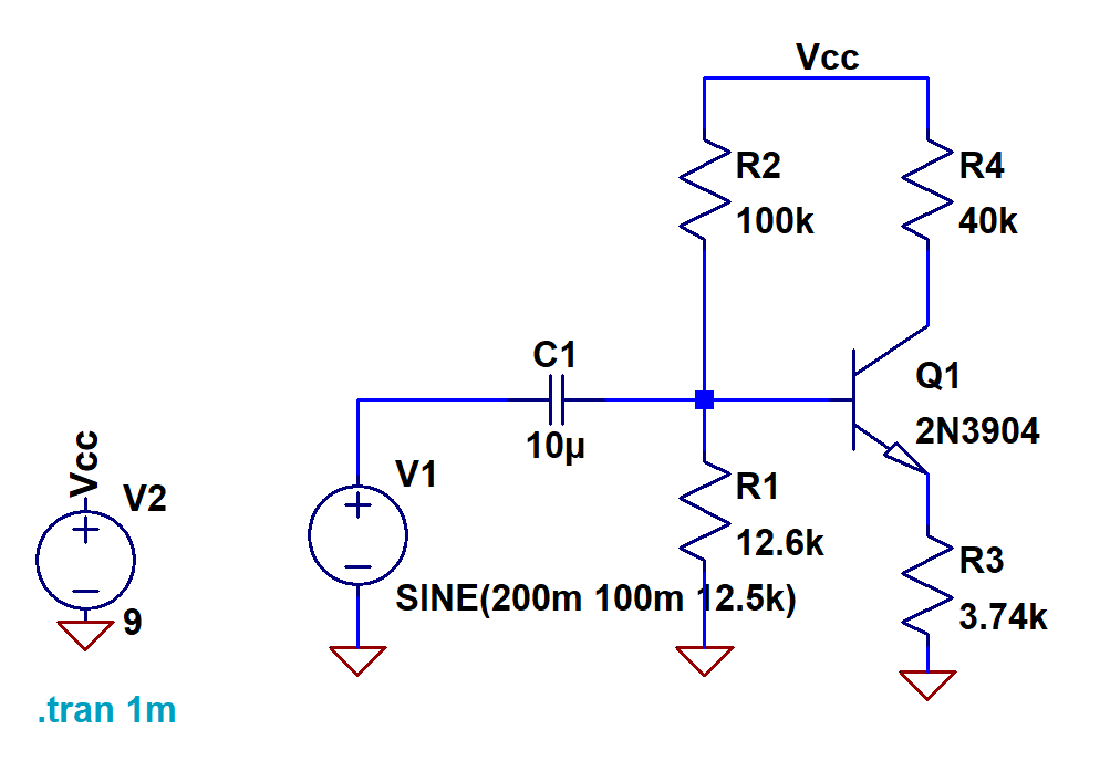
Beautiful. Now we didn’t really go into choosing the coupling capacitor, because it doesn’t quite matter in this situation. We make it large enough so that it’s not attenuating our input signal. 10uF is a typical value for a scenario like this. Now we have a circuit, we have components, topology, values, and signals, we can run a simulation.
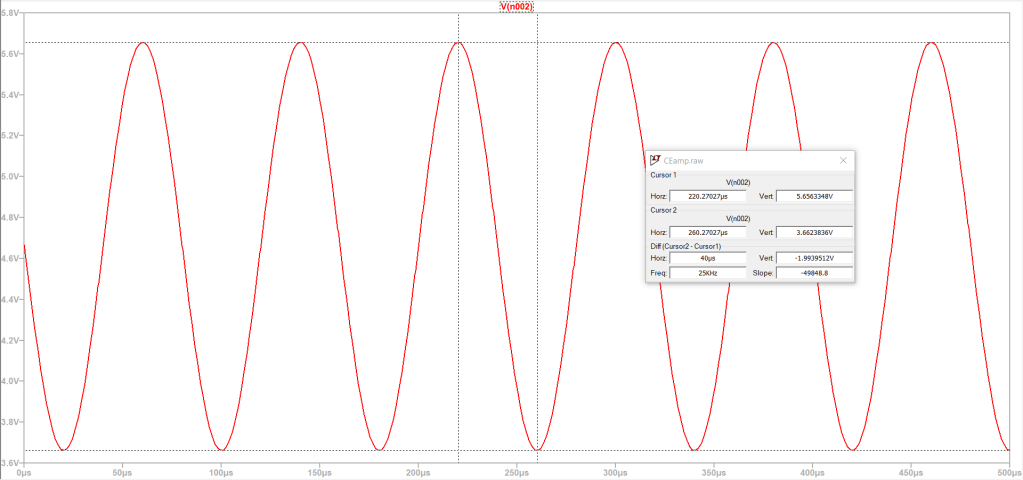
Okay so what’s wrong and what’s right? We can see the signal gain is pretty much perfect. We input 200mVpp, and we get 2Vpp output, which means we got our gain of 10 dead on. The DC offset is wrong though. Instead of being centered around 5V, it’s centered around 4.7V. That’s likely because we used an Is and Beta lower than what this model uses.
Now, we could start tweaking values here to get this just right, but we’re trying to build a physical circuit. In the end we’ll have to use real components with fixed discrete values. We might adjust 12.6kOhm to be 12.5kOhm but guess what, I don’t have a 12.6kOhm or 12.5kOhm resistor on me. I have to take the resistors I do have and get as close as possible. These are the constant sacrifices in COTS (commercial off-the-shelf) engineering. You have to work with what you have available. After looking through what I have on me, this is what I’ve come up with.
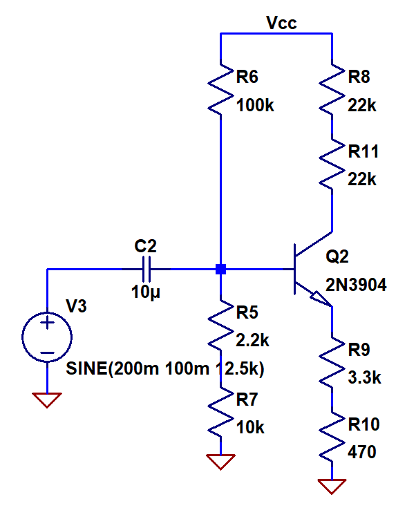
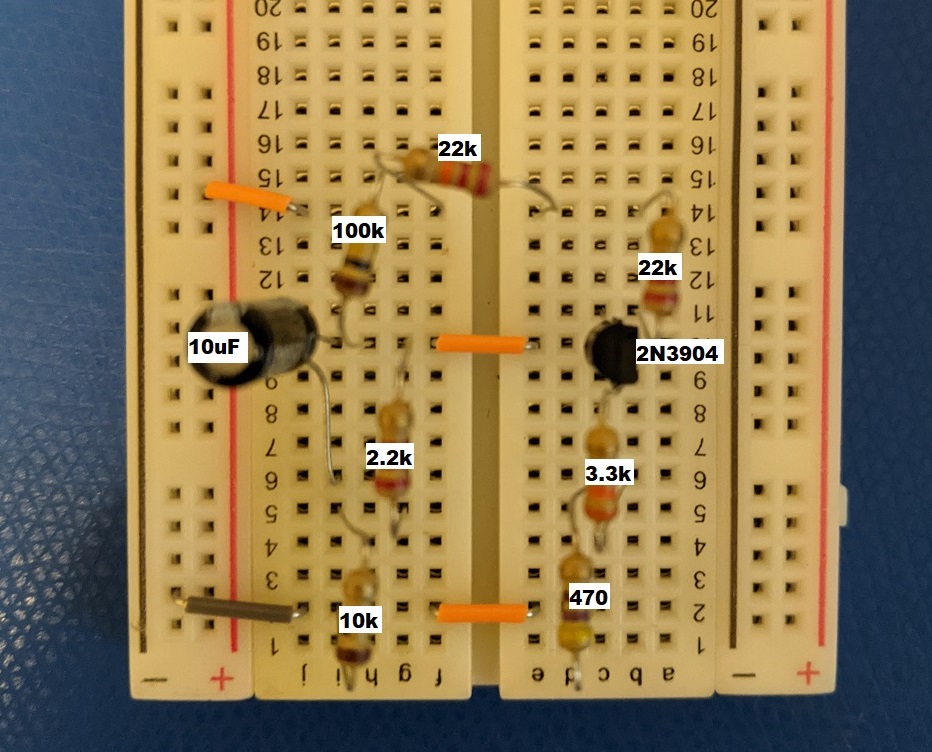
The lowering of Rb2 is the biggest difference. From 12.6kOhm to 12.2kOhm. That could be a really good thing though, since we underestimated Is and Beta. And here it is laid out on the breadboard!
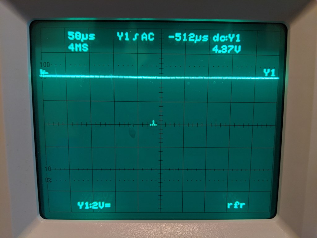
We first hook up the power source, our 9V battery, to get an idea of the output bias. My oscilloscope shows the collector voltage is 4.37V. It’s not great, it’s too low. The collector voltage is pushed lower by more current running through the Rc. I thought lowering Rc and Rb2 would offset our approximations but our 2N3904 is performing better than we expected. I’m really happy for him, he’s showing off his best, but that extra effort screwed with our careful calculations.
What’s our output waveform look like? Well let’s see what the oscilloscope shows, input and output side by side.
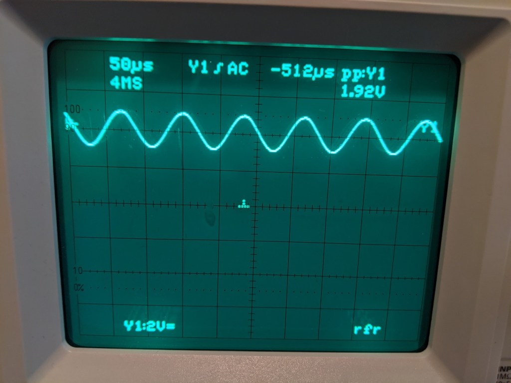
What happened here, where did we fail? The input is 200mV, why isn’t the output 2V? In fact, if we have a larger collector current (if the output DC is lower, by Ohm’s law that means the current across Rc is greater), why isn’t the small signal gain greater? After all, the small signal gain gm=Ic/Vt.
The answer is in that second variable, Vt. Vt is the thermal voltage. It’s a measure of statistical activity and energy of electrons. Sort of how the resistance of an object increases as its temperature goes up, because more energy is lost to particle collisions, the “resistance” of the BJT semiconductor goes up as its temperature goes up. Our calculations assumed a room temperature Vt of 26mV, but in reality it’s going to be higher.
So why is the temperature higher than room temp? Two reasons. One, it is a hot June summer day and I’m in a small room without air conditioning. Send help. Two, the moment the BJT conducts current, it begins dissipating heat and its temperature rises.
That first point sounds like a joke but it’s actually a very important consideration. When Apple makes an iPhone, they don’t sell you one to use in winter where you’re calling for a cab when it’s freezing outside, and one to use in summer where you’re using GPS walking on scorching pavement. They don’t sell different iPhones that only work in frigid Stockholm and ones that only work in humid Mumbai. Believe me, they would if they could. The ambient temperature could be anywhere from -35C up to +35C. In Kelvin you’re looking at a 20%+ variation in temperature, which means a 20%+ variation in the thermal voltage.
The design must account for this, which is no device you buy uses just a mere single transistor amplifier. They use several blocks with more complex biasing systems, and lots of feedback and control loops, all meant to ensure as deterministic operation as possible across all use cases. But, at the heart of any amplifier contains all the concepts we just covered here in this single transistor amplifier.

One thought on “BJT Amplifier – Concept to Components”