I started a Master’s program in Fall 2021, and my first class was EECE 5649, Design of Analog Integrated Circuits with CMOS Technology. Instead of a final exam, we were assigned a term project that we completed in teams of 3 over the course of a month. The professor gave us a list of 4 projects we could pick from, and if we wanted we could also come up with our own project or try a variation of one from the list with approval. The 4 projects were: a bandgap reference, instrumentation amplifier for EEG signals, sine wave generator, or transimpedance amplifier for an optical receiver. We ended up choosing the instrumentation amplifier. The prompt was as follows:
Instrumentation amplifiers are critical components in analog front-ends for electroencephalography (EEG) signal recording devices. As part of this project, review the different design approaches and performance state-of-the-art for CMOS instrumentation amplifiers. Select a circuit architecture with which you expect excellent performance in 180nm CMOS technology, and design it with the goal to optimize performance using a 0.2pF load capacitance. You may explore modifications of the initial amplifier circuit to improve it. Compare the simulation results in a summary table with simulation/measurement results from at least 8 IEEE journal or conference papers (preferably published within the last 4 years). Compare all relevant specifications in the table, including (but not limited to) gain, bandwidth, power consumption, total harmonic distortion, output offset voltage (with 100 Monte Carlo simulations from schematic simulations), input-referred noise, common-mode rejection ratio (with 100 Monte Carlo simulations from schematic simulations), power supply rejection (with 100 Monte Carlo simulations from schematic simulations), power supply voltage. Present the results with the same format/convention as in the reference papers. Layout is required for this project. Report the total layout area, and list it in the comparison table.
Right-o, let’s begin! Let’s lay out our broad requirements. The first stage was research, where we read through IEEE papers on other peoples’ efforts in instrumentation amplifier design in sub-micron CMOS technology. That allowed us to get a feeling of what expectations were, what were reasonable design specs to hit. Discrete instrumentation amplifiers have the advantage of being based on older more reliable fabrication technology, so looking at what teams are able to accomplish at on-chip 45nm gave us a fair comparison.
For those unfamiliar, an instrumentation amplifier is a configuration of multiple op-amps that is meant to amplify small sensor signals that may be mired in noise and have a DC offset. Below on the left is a figure showing how a discrete monolithic instrumentation amplifier would be connected in a circuit. The positive and negative inputs are connected to each half of a Wheatstone bridge, where they both see a common DC offset when the signal is 0, but when either resistor changes value (with one of the resistors representing something like a strain gauge that changes resistance based on pressure), a small difference appears between the two terminals.
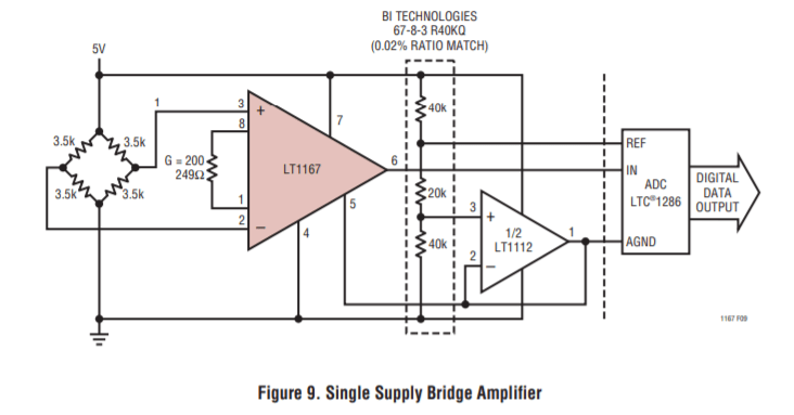
The figure on the right is the classical instrumentation amplifier configuration. The first two op-amps at the input provide two things: a high input impedance, and high gain. The third op-amp is a differential amplifier, and provides high common-mode rejection, getting rid of any DC offset.
We did some research on different topologies beyond the classical configuration. There’s been a few improvements recently, primarily the explosion of switched-capacitor circuits. Digital control of switches charging capacitors allow implementation of all sorts of mathematical functions like filtering, programmable impedance, auto-nulling, and more. Being digital, this was entirely out of our purview, so we went with the classical topology.
There were three main stages to the design from a schematic point. Stage 1: the biasing. Stage 2: the op-amp. Stage 3: the full amplifier.
The biasing took very little time because we simply had no bandgap reference available. There just wasn’t much to do here but to create a create mirror, and program it with a resistor from an ideal Vdd. The main thing to be concerned about was process variance and noise. The power supply was allowed to be modeled as an ideal source for this project, so we didn’t have to worry about that, but any noise from any part of the biasing circuitry would go down the entire line. For a MOSFET, that basically means go big or go home. Increasing the area evens out the variations in the silicon wafer, and it keeps the noise low.

Next part….the op-amp. I can’t believe I’m just saying it like it’s nothing. I have nothing but infinite respect for anyone who does this for a living. Op-amps usually have an OTA (operational transconductance amplifier) at their heart, followed by an output stage, and maybe an extra amplification stage. The OTA can have a differential output or single ended, it can be cascoded, and it can optimize gain or stability or bandwidth etc. So many choices.
We decided to do a standard single-ended output OTA going into a common-source amplifier output stage mostly because it couple provide reasonably high gain while also having fewer transistors to fiddle with. We also decided to make it a PMOS amplifier going into a NMOS CS stage because noise is dependent on carrier mobility, and PMOSes have a lower mobility just by virtue of being majority hole carrier.

Now here’s a lesson we wish we had properly learned before we started designing the op-amp. Op-amps that are meant to be part of a whole other IC have much different requirements than a discrete op-amp you’d buy off Digikey. So misguidedly, we spent a lot of time trying to hit open-loop gains of 80dB. That’s a stupid thing to do because you get absolutely no stability. But also at the same time, loop stability doesn’t really matter for the single op-amp here, because we’re connecting it in an instrumentation configuration.
See, with a discrete op-amp, or discrete instrumentation amplifier, the end user will be using it in a variety of different ways. They might be using the op-amp to provide a voltage reference, or be part of a filter, or output current, or drive a large capacitive load. Weirdly, the designer is constrained by the freedom of the end user. Here that’s not the case. We know exactly how it’s going to be used, it’s going in an IC that nobody can change. Also, discrete amplifiers use older technologies with larger transistors that don’t suffer from short-channel effects.
Not knowing this ended up with us failing at getting high gain, then ruining our stability, over and over and over. Once we got it to a point we were okay with, we put it into the instrumentation amplifier configuration and everything broke again. We never needed that much gain. The point of the instrumentation amplifier was to take a 10uV signal and amplify it to about 10mV or so (that’s 60dB *total* while we achieved over 90dB for a single op-amp), and mostly just get rid of the common-mode and noise, so that the next stage in the IC could work with a clean easy signal.
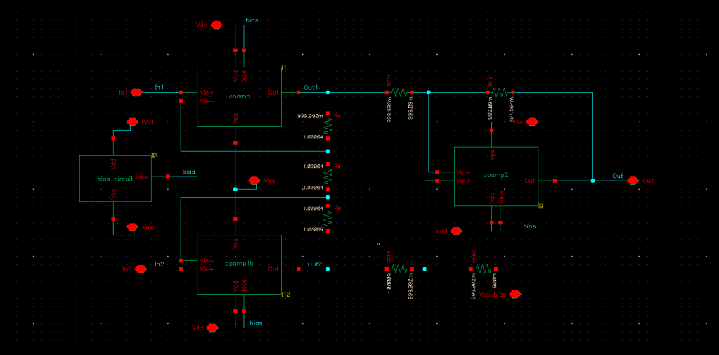
Here below is the schematic with the op-amps all wired up in the instrumentation configuration.
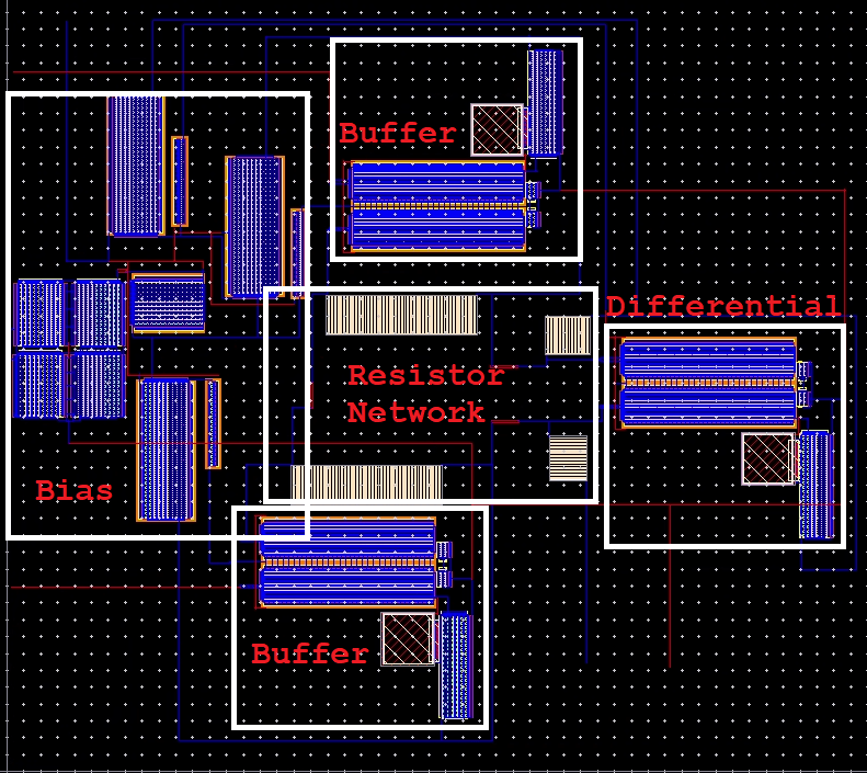
And then here is the layout. Fortunately there was no requirement to optimize layout, just to get it done, extract parasitics, and provide simulation results to explain how and why the parasitics affected the outcome.
If you’d like a personal insight into what it’s like going through this class and designing an amplifier in Cadence for the first time, I wrote a war story about it in the blog section.
